Passivation contact cell and preparation method thereof, and passivation contact structure preparation method and device
A contact structure and battery technology, applied in the field of solar cells, can solve the problems of longer heating time, cooling waiting time, inconsistent process temperature, and increased winding plating steps, so as to reduce post-cleaning steps, no winding plating, and improve electrical performance. Effect
- Summary
- Abstract
- Description
- Claims
- Application Information
AI Technical Summary
Problems solved by technology
Method used
Image
Examples
preparation example Construction
[0062] The invention provides a method for preparing a passivated contact structure, comprising the following steps:
[0063] S1. First place the substrate in a PECVD process chamber to deposit a tunneling oxide layer, and then place it in a PVD process chamber to deposit a doped amorphous silicon layer; the PECVD process chamber is provided with a first gas, and the PVD process chamber A second gas and a target are arranged inside;
[0064] The target material includes at least one target material containing a dopant source, and the second gas does not contain a dopant source gas; or,
[0065] The target material includes at least one target material containing a dopant source, and the second gas includes a dopant source gas; or,
[0066] The target material does not contain a target material containing a dopant source, and the second gas contains a dopant source gas;
[0067] The doped amorphous silicon layer includes an n-layer thin film, n≥2, and the n-layer thin film in...
Embodiment 1
[0105] This embodiment describes in detail the preparation method of the passivation contact structure.
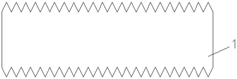
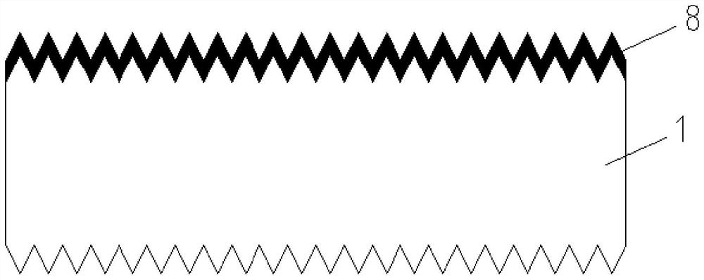
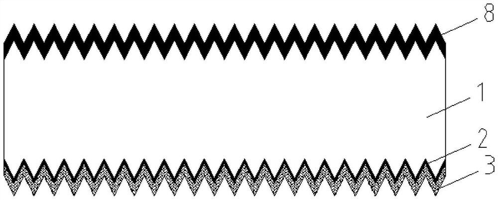
[0106] Step S0 , select an N-type substrate 1 and perform pretreatment on the substrate to form a textured structure on the surface of the substrate. The resistivity of the n-type crystalline silicon substrate is 0.3-5 Ω·cm, and the thickness is 80-200 μm.
[0107] Step S1, put the substrate 1 pretreated in step S0 into the loading chamber for loading, and enter the PECVD process chamber. In the PECVD process chamber, a tunneling oxide layer 2 is generated by plasma excitation. The gas introduced into the PECVD process chamber is Oxygen; after the deposition of the tunneling oxide layer 2 is completed in the PECVD process chamber, the substrate enters the PVD process chamber. The PVD process chamber includes two independent chambers. The process chamber is filled with argon gas. Silicon pillar target material, the second chamber is equipped with a target material containin...
Embodiment 2
[0110] This embodiment describes in detail the preparation method of the passivation contact structure.
[0111] Step S0, select the P-type substrate 1, and pretreat the substrate to form a textured structure on the surface of the substrate. The resistivity of the n-type crystalline silicon substrate is 0.1-5Ω·cm, and the thickness is 80-200μm.
[0112] Step S1, put the substrate pretreated in step S0 into the loading chamber for loading, and enter the PECVD process chamber, and generate a tunneling oxide layer 2 through plasma excitation in the PECVD process chamber, the thickness of which is 0.5-3nm, and the PECVD process chamber The gas introduced into the interior is oxygen; after the deposition of the tunneling oxide layer 2 is completed in the PECVD process chamber, the substrate enters the PVD process chamber. The PVD process chamber includes two independent chambers, and argon gas is introduced into the process chamber. A pure silicon column target is set in the cavity...
PUM
| Property | Measurement | Unit |
|---|---|---|
| thickness | aaaaa | aaaaa |
| electrical resistivity | aaaaa | aaaaa |
| thickness | aaaaa | aaaaa |
Abstract
Description
Claims
Application Information


