Method for improving electroforming thickness uniformity of wafer-level array microstructure

A technology with uniform thickness and array structure, applied in electrodes, circuits, semiconductor devices, etc., can solve the problems of uneven current density distribution, affecting the efficiency of electroforming process, low electroforming efficiency, etc., to solve the problem of edge effect and microstructure. And performance consistency guarantee, the effect of simple installation

Active Publication Date: 2022-03-01
NANJING UNIV OF AERONAUTICS & ASTRONAUTICS
View PDF11 Cites 0 Cited by
  • Summary
  • Abstract
  • Description
  • Claims
  • Application Information

AI Technical Summary

Problems solved by technology

Unfortunately, shortening the pulse interval to the millisecond range severely compromises the efficiency of the electroforming process
At the same time, the application of reverse pulse current also faces the problem of uneven current density distribution, which limits the application of this technology in wafer array microstructure electroforming
It can be seen that although the existing improved methods have improved the uniformity of the electroforming layer to a certain extent, the disadvantages of low electroforming efficiency and poor versatility still exist, which limit its application in actual production, so a A Novel Method for Improving Thickness Uniformity of Electroformed Microstructures in Wafer-Level Arrays

Method used


Image

  • Method for improving electroforming thickness uniformity of wafer-level array microstructure
  • Method for improving electroforming thickness uniformity of wafer-level array microstructure
  • Method for improving electroforming thickness uniformity of wafer-level array microstructure

Examples


Embodiment 1

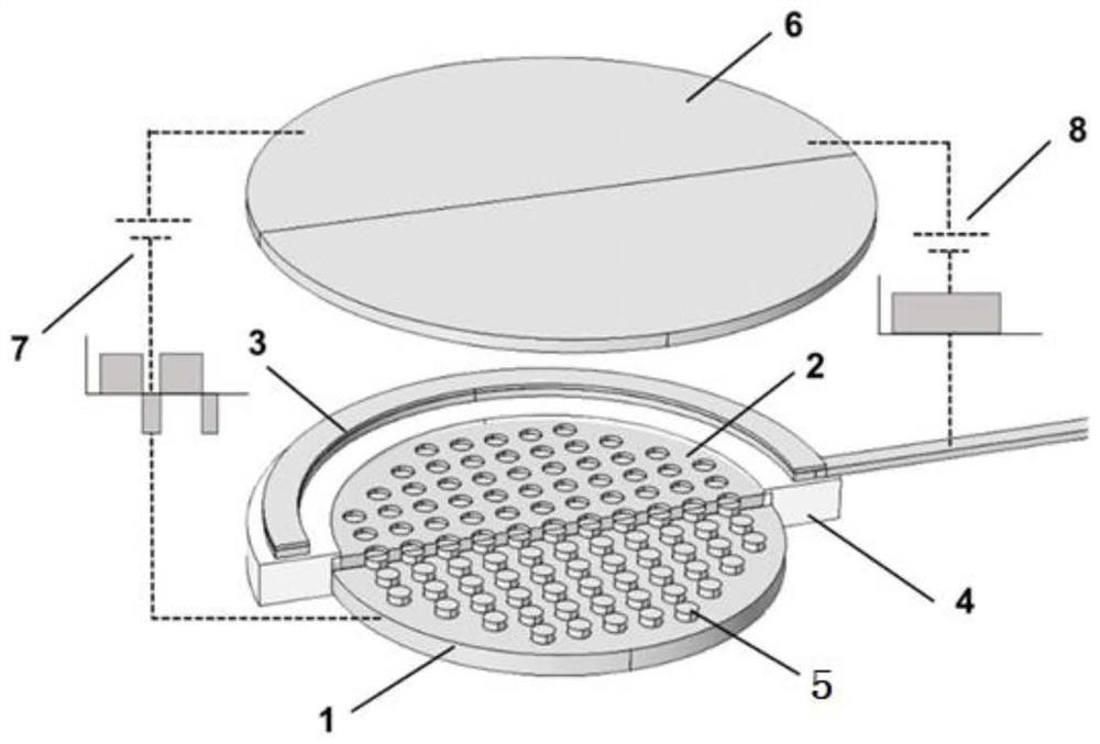
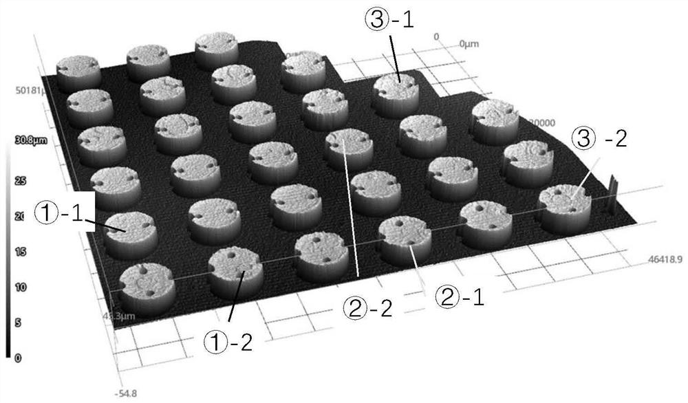
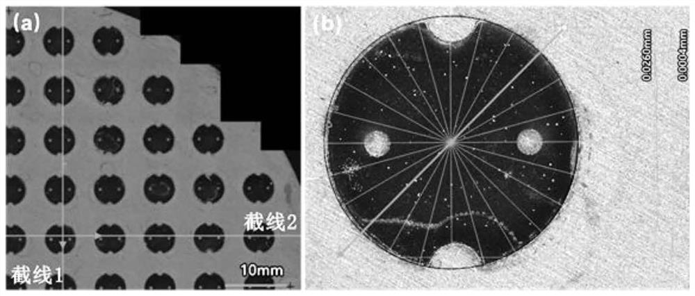
[0036] On the cathode of a 4-inch mirror stainless steel wafer, an array structure of copper circles with a thickness of 25 microns is electroformed, such as figure 1 shown, including the following steps:

[0037] Step a), wafer cathode pre-treatment: first use acetone and alcohol to degrease the 4-inch (diameter 101.6mm) wafer cathode, then rinse with deionized water, dry it with nitrogen, and put it in an oven at 90°C Bake in medium for 15 minutes, take out and cool to room temperature;

[0038] Step b), electroforming film production: coating a liquid SU-8 photoresist with a thickness of 35 microns on the wafer cathode and standing for 15 minutes; pre-baking parameters: 95 ° C for 5 minutes; exposure dose 300mj / cm 2 , the time is 7 seconds; post-baking parameters: 95 ° C for 30 minutes; development: put it in SU-8 developer and let it stand for 5 minutes; take it out and clean it to get the required array structure film;

[0039] Step c), microstructure electroforming:

...


PUM

PropertyMeasurementUnit
sizeaaaaaaaaaa
diameteraaaaaaaaaa
thicknessaaaaaaaaaa

Abstract

The invention discloses a method for improving the uniformity of the electroforming thickness of a wafer-level array microstructure, and the method comprises the steps: guaranteeing the consistency of the surface current density distribution of the whole array microstructure through installing an auxiliary cathode at the periphery of a wafer cathode and applying a direct current; and meanwhile, the reverse pulse current is applied to the surface of the wafer cathode to perform electrochemical micro-leveling on the microstructure unit in the array, and based on the high synergistic effect of the auxiliary cathode and the reverse pulse current, the uniformity of the electroforming thickness of the wafer-level array microstructure is improved. The method overcomes the defects that an existing method is poor in universality, low in machining efficiency and the like, avoids the edge effect problem in a traditional electroforming process and the problem of low deposition rate in a reverse pulse electroforming process, and can obtain a microstructure electroforming layer which is uniform in thickness and good in organization structure and performance consistency on the surface of a 4-6 inch wafer at the high current density of 2-8 A / dm < 2 >; and the auxiliary cathode can be repeatedly used, and the method is simple and easy to implement and has higher practicability.

Description

technical field [0001] The invention relates to the field of micro-manufacturing technology, in particular to a method for improving the thickness uniformity of wafer-level array microstructure electroforming. Background technique [0002] With the development of micro-electromechanical systems (MEMS) technology, electroforming technology, as an important micro-fabrication method, has been widely used in aerospace, precision machinery, biomedicine, communication and other fields. Most of the current work related to the electroforming process uses a small-area wafer substrate as the cathode to fabricate microstructures, which limits the number of layouts of micropatterns on the substrate, thereby affecting production efficiency. In addition, the current density distribution on the cathode surface is not uniform in the process of making micro devices by electroforming technology, and the problem of inconsistent thickness between the edge area and the middle area of ​​the elect...

Claims


Application Information

Patent Timeline
Patent Type & Authority Applications(China)
IPC IPC(8): C25D7/12C25D5/02C25D5/18C25D17/10
CPCC25D7/12C25D5/022C25D5/18C25D17/10Y02P70/50
Inventor 朱增伟詹晓非
Owner NANJING UNIV OF AERONAUTICS & ASTRONAUTICS
Why Eureka
Try Eureka