Symmetrically-arranged full-bridge power module

A power module and symmetrical technology, which is applied in the field of power semiconductor devices, can solve the problems of switching oscillation and high turn-off voltage, and achieve the effect of reducing switching oscillation, reducing parasitic inductance, and achieving symmetry

Pending Publication Date: 2022-03-01
HUAZHONG UNIV OF SCI & TECH
View PDF0 Cites 0 Cited by
  • Summary
  • Abstract
  • Description
  • Claims
  • Application Information

AI Technical Summary

Problems solved by technology

[0005] The present invention provides a full-bridge power module with a symmetrical layout, which is used to solve the technical problems that the existing full-bridge power module has a large parasitic inductance value due to its structural layout, which leads to excessively high turn-off voltage and serious switching oscillations

Method used


Image

  • Symmetrically-arranged full-bridge power module
  • Symmetrically-arranged full-bridge power module
  • Symmetrically-arranged full-bridge power module

Examples


Embodiment 1

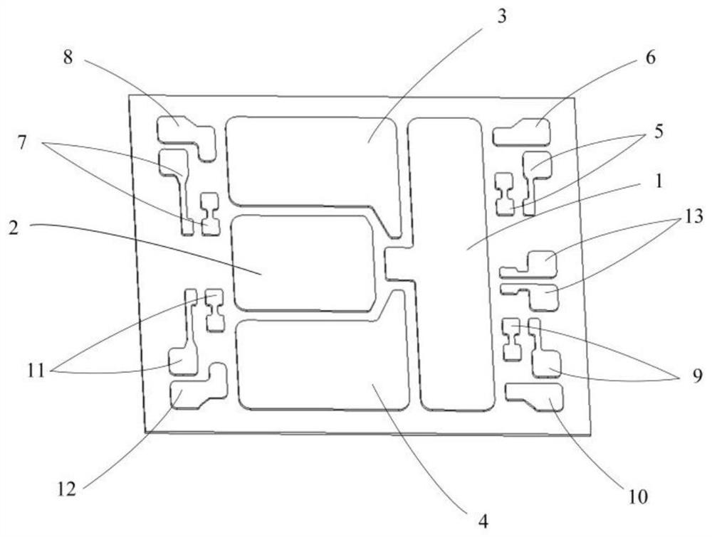
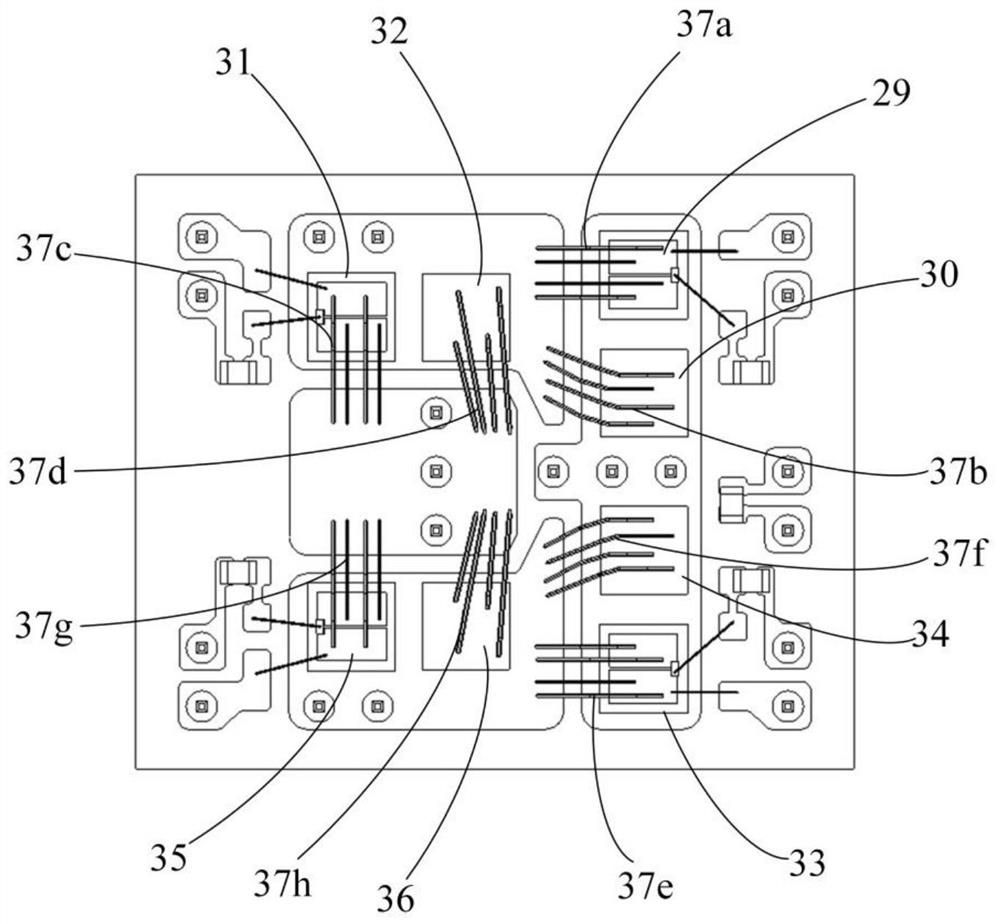
[0034] A full-bridge power module with a symmetrical layout. The full-bridge power module includes insulating substrates, power chips (including switch tube chips and diode chips), terminals and other parts; the insulating substrate is divided into upper surface metal layer, middle insulating layer and The metal layer on the lower surface and the metal layer on the upper surface include: positive electrode metal layer, negative electrode metal layer, first AC electrode metal layer, second AC electrode metal layer and each copper layer for driving signal connection; first AC electrode metal layer, The negative electrode metal layer and the second AC electrode metal layer are arranged laterally in sequence, and all three are adjacent to the positive electrode metal layer; the positive electrode metal layer and the negative electrode metal layer are respectively symmetrical about the central axis, and the first AC electrode metal layer and the second AC electrode metal layer The l...

Embodiment 2

[0060] The power module of the above-mentioned embodiment 1 can realize the topology of the full-bridge rectifier circuit after removing the switching tube chip and keeping only the diode chip; similarly, the working conditions and service life of the diode chips on the four bridge arms can be kept consistent.

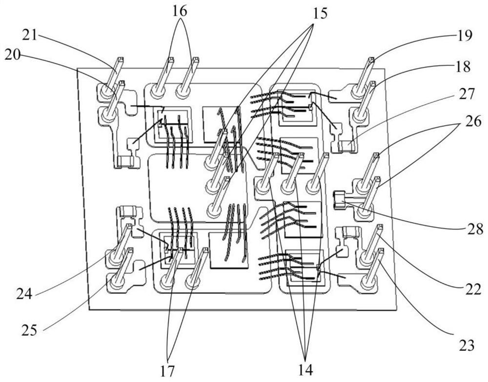
[0061] like Image 6 and Figure 7 Shown is a full-bridge rectifier module applying this full-bridge module layout. Similarly, as another example of the present invention, the number of parallel diode chips of each bridge arm is 1; the insulating substrate adopts a direct copper-clad ceramic board (DBC), the corresponding metal layers are copper layers, and the intermediate layer adopts aluminum nitride Ceramic; features pin terminals.

[0062] Image 6 It is a schematic diagram of the internal structure of a full-bridge rectifier module with a symmetrical layout. The arrangement of the copper layer on the upper surface of the insulating substrate is the same as th...


PUM


Abstract

The invention belongs to the technical field of power semiconductor devices, and particularly discloses a symmetrically-arranged full-bridge power module, and power chips form four bridge arms of a full-bridge circuit topology; the back surfaces of the power chips forming the two upper bridge arms are welded on the positive electrode metal layer of the insulating substrate, and the front surfaces of the power chips are connected with the corresponding metal layers of the insulating substrate through bonding wires; the back faces of the power chips forming the two lower bridge arms are welded to the two alternating current electrode metal layers of the insulating substrate, the front faces of the power chips are connected with the corresponding metal layers of the insulating substrate through bonding wires, and switch tube driving circuits of the power chips are connected through Kelvin. According to the power module, after the switch tube chip is removed and only the diode chip is reserved, the full-bridge rectification circuit topology can be realized. Through layout design of the copper layers, the power devices and the terminals, symmetry between the two half-bridge branches and symmetry between the two commutation loops of the same half-bridge branch are achieved, a small parasitic inductance value is achieved, and turn-off overvoltage and switch oscillation are reduced.

Description

technical field [0001] The invention belongs to the technical field of power semiconductor devices. More specifically, it relates to a symmetrical layout of a full-bridge power module. Background technique [0002] With the rapid development of modern transportation, aerospace and other fields, power electronic power modules have been widely used. Higher requirements are also placed on the performance of power electronic power modules. [0003] Most of the existing power modules adopt the wire bonding process, and the connection of the top electrodes of the power chip is realized through the bonding wire. The geometric size of the chip itself and the limitation of the internal bonding wire connection of the power module will make the parasitic inductance parameter inside the module larger, which makes the switch tube chip withstand a large peak voltage when it is turned off at high speed, and the switching transient occurs Larger oscillations. These effects will be more ...

Claims


Application Information

Patent Timeline
Patent Type & Authority Applications(China)
IPC IPC(8): H01L25/07H01L25/00H01L23/58H01L23/48
CPCH01L25/071H01L25/50H01L23/58H01L23/481H01L2224/48227H01L2224/0603H01L2224/49111
Inventor 陈材吕坚玮黄志召刘新民康勇
Owner HUAZHONG UNIV OF SCI & TECH
Why Eureka
Try Eureka