Laser power stabilization system based on FPGA and liquid crystal TNE effect
A laser power and stable system technology, applied in the direction of lasers, laser components, phonon exciters, etc., can solve the problems of inability to complete high-speed calculations at the same time, and slow response speed of liquid crystals in power stabilization systems, so as to improve the response speed of liquid crystals and improve The effect of high frequency response
- Summary
- Abstract
- Description
- Claims
- Application Information
AI Technical Summary
Problems solved by technology
Method used
Image

Examples
Embodiment Construction
[0023] The present invention will be further described below in conjunction with the accompanying drawings and specific implementation methods.
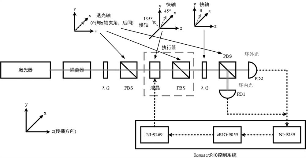
[0024] Based on the NI CompactRIO system, the present invention proposes a new laser power stabilization system. The 1.33Ghz dual-core processor of the Linux RT system runs on the CompactRIO system, and is equipped with a programmable FPGA chip. Therefore, each input and output module of the system is directly connected to the FPGA chip, rather than through a bus connection, so the system response of CompactRIO has almost no delay compared with other controller architectures.
[0025] In addition, compared with the traditional control system developed based on FPGA chips, the LabVIEW FPGA software installed in CompactRIO has a better graphical interactive interface, which can process and display graphics in real time. At the same time, the system also has 2GB of DRAM and 4GB of storage space , very suitable for real-time data proces...
PUM
 Abstract
Description
Claims
Application Information
PatSnap Eureka turns technology decisions into work you can execute. Powered by our Innovation Knowledge Graph, it runs expert workflows across engineering, life sciences, materials and intellectual property. Get your review-ready output in minutes.


