
Terahertz modulator with cavity loading resonance unit nested diode

A resonant unit and diode technology, applied in the direction of instruments, nonlinear optics, optics, etc., can solve the problem that the modulation rate is difficult to increase, and achieve the effects of reducing complexity, increasing modulation depth and modulation rate, and suppressing leakage

Pending Publication Date: 2022-03-11
上海微波技术研究所(中国电子科技集团公司第五十研究所)
View PDF1 Cites 0 Cited by
  • Summary
  • Abstract
  • Description
  • Claims
  • Application Information

AI Technical Summary

Problems solved by technology

However, this patent document still has the defect that the modulation rate is difficult to increase

Method used


Image

  • Terahertz modulator with cavity loading resonance unit nested diode
  • Terahertz modulator with cavity loading resonance unit nested diode
  • Terahertz modulator with cavity loading resonance unit nested diode

Examples


Embodiment 1

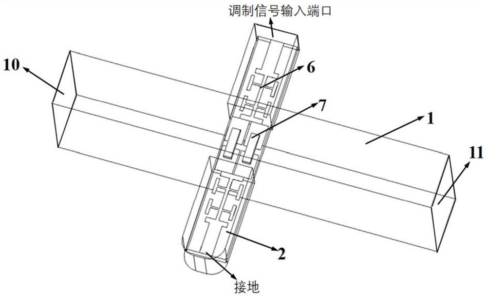
[0044] Such as figure 1 with figure 2As shown, this embodiment provides a terahertz modulator with diodes embedded in a cavity-loaded resonant unit, including a rectangular waveguide 1 and a modulation chip 2 , and the modulation chip 2 is arranged on the cavity wall of the rectangular waveguide 1 . The rectangular waveguide 1 is provided with an input waveguide port 10 and an output waveguide port 11. The plane where the modulation chip 2 is located is perpendicular to the input waveguide port face 10 and the output waveguide port face 11. The modulation chip 2 includes a semiconductor substrate 3 and a surface placed on the semiconductor substrate 3. The artificial microstructure on the surface, one side of the semiconductor substrate 3 is in contact with the cavity wall of the rectangular waveguide 1, the artificial microstructure is not in contact with the cavity wall of the rectangular waveguide 1, and the vertical upper and lower side walls of the rectangular waveguide ...

Embodiment 2

[0048] Those skilled in the art can understand this embodiment as a more specific description of Embodiment 1.

[0049] Such as figure 1 with figure 2 As shown, this embodiment provides a terahertz modulator with diodes embedded in a cavity-loaded resonant unit, including a rectangular waveguide 1 and a modulation chip 2 .

[0050] The rectangular waveguide 1 has two waveguide ports, input and output, which are respectively the input waveguide port 10 and the output waveguide port 11, and its cavity wall is made of metal material, and the metal material of the rectangular waveguide cavity wall is oxygen-free copper, brass or aluminum; The modulation chip plane is perpendicular to the rectangular waveguide opening; the modulation chip includes a semiconductor substrate 3 and an artificial microstructure placed on the semiconductor substrate, the semiconductor substrate side of the modulation chip is connected to the wall of the rectangular waveguide cavity, and the artificial...

Embodiment 3

[0056] Those skilled in the art can understand this embodiment as a more specific description of Embodiment 1.

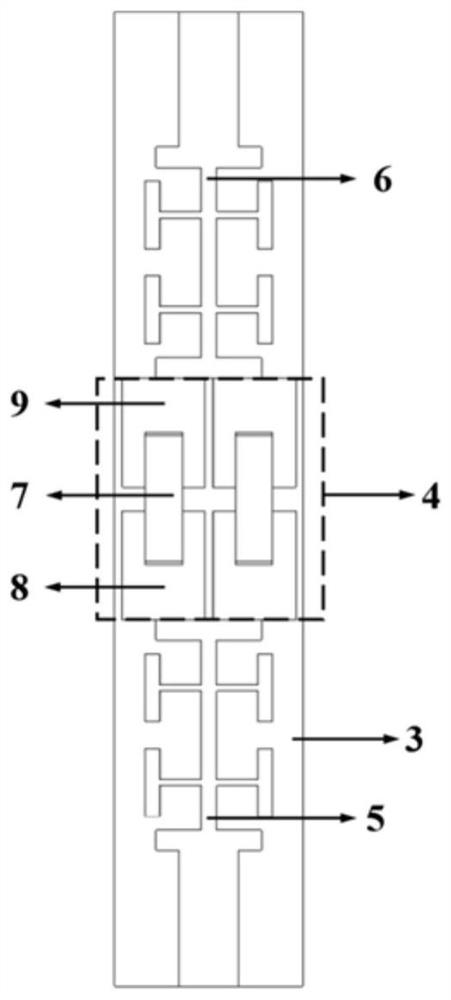
[0057] Such as Figure 1~4 As shown, this embodiment provides a terahertz modulator with diodes embedded in a cavity-loaded resonant unit, including a rectangular waveguide 1 and a modulation chip 2 . The modulation chip 2 includes a semiconductor substrate 3 , a modulation array 4 , a ground structure 5 and a filter feed structure 6 . The modulation array 4 , the ground structure 5 and the filter feed structure 6 form a metal layer structure, and the metal layer is grown on the semiconductor substrate 3 .

[0058] The modulation array is two modulation units in a single row, the modulation units are connected in parallel, and the cathode resonators of the two modulation units are connected to the same grounding structure, and the anode resonators of the two modulation units are connected to the same filtering structure for external The feed-in of the voltage sign...


PUM


Abstract

The invention provides a terahertz modulator with a cavity loading resonance unit nested diode, which comprises a rectangular waveguide and a modulation chip, and is characterized in that the modulation chip is arranged on the cavity wall of the rectangular waveguide; the rectangular waveguide is provided with an input waveguide port and an output waveguide port. The modulation chip comprises a semiconductor substrate and an artificial microstructure arranged on the semiconductor substrate; one side of the semiconductor substrate is in contact with the cavity wall of the rectangular waveguide, and the artificial microstructure is not in contact with the cavity wall of the rectangular waveguide; the longitudinal upper and lower side walls of the rectangular waveguide are in contact with the modulation chip and are respectively provided with an air window, and the air windows are used for electrically connecting an external control circuit with electrodes on the chip. The artificial microstructure on the modulation chip adopts a few modulation units, compared with a traditional large array design, a parasitic mode existing in a large array structure is effectively restrained, the high-frequency characteristic of a diode in the chip can be brought into play, and therefore the modulation rate of a device is improved.

Description

technical field [0001] The present invention relates to the technical field of electromagnetic functional devices, in particular to a terahertz modulator in which a diode is embedded in a cavity-loaded resonant unit. Background technique [0002] Due to the frequency band and inherent characteristics of terahertz waves, terahertz scientific research has important application value in medical treatment, detection, imaging, wireless communication and other fields. Among them, wireless communication is an important development direction in the field of electronic information. Terahertz communication has the advantages of combining microwave communication and optical communication, and has become the key to wireless communication close to the wired data rate. Compared with millimeter-wave frequency bands, terahertz communication has larger transmission bandwidth and higher security performance. Compared with other frequency bands, terahertz communication is easier to track and ...

Claims


Application Information

Patent Timeline
IPC IPC(8): G02F1/01
CPCG02F1/011G02F2203/13
Inventor 郭小庆王晓东马维一崔慧源李云云
Owner 上海微波技术研究所(中国电子科技集团公司第五十研究所)
Learn More