
Eureka
For R&D, Eureka makes reading and utilizing patents & technical documents easy.
Eureka AIR
Designed for self-driven R&D workflows. Generate viable solutions, solve complex R&D challenges, empower your innovation with AI.

Eureka Materials
Designed for material experts only. Revolutionize your material R&D, from search, analyze, to developing new materials.

TechResearch
Generate reliable direction feasibility study reports for your R&D in just a few steps.

TechSeek
Discover and master advanced knowledge NOW. Basics, ideas, possibilities, all at once.

TechMind
As an expert in R&D Theories, TechMind can generates customized viable solutions instantly.

TechRisk
Analyze your overall solution with one click, know your potential R&D risks in advance.

TechMonitor
Get weekly tech updates, stay abreast of the latest tech innovations and key insights.
Preparation method of high-speed photoelectric detector chip
A photodetector and chip technology, applied in circuits, electrical components, semiconductor devices, etc., can solve problems such as excessive window size, decreased responsivity, and reduced photosensitive surface, achieving high response rate and reducing capacitance.
- Summary
- Abstract
- Description
- Claims
- Application Information
AI Technical Summary
Problems solved by technology
Method used
Image

Examples
Embodiment Construction
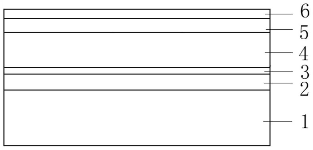
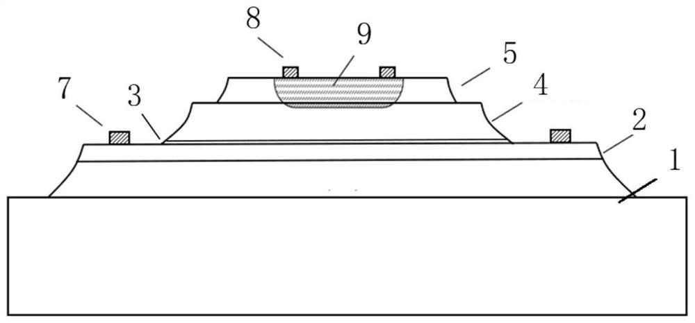
[0041] see figure 1 with figure 2 , a high-speed photodetector chip provided by an embodiment of the present invention includes a substrate 1 and an epitaxial layer grown on the substrate 1, wherein the epitaxial layer includes an N-type InGaAs contact layer 2 from bottom to top, an InP etch stop layer 3. InGaAs absorption layer 4, InGaAsP transition layer 5, and InGaAs contact layer 6.
[0042] Further, a high-speed photodetector chip provided by an embodiment of the present invention further includes an N electrode 7 disposed on the N-type InGaAs contact layer 2 , and a P electrode 8 disposed on the InGaAs contact layer 6 . In the present invention, the N electrode is arranged on the N-type contact layer made of InGaAs material. Since the forbidden band width of the InGaAs material is 1.43eV~0.35eV, the N-type InGaAs contact layer can be directly connected with the Ti-Pt-Au metal forming the N electrode. layer forms a good metal-semiconductor contact. In the chip prepar...
PUM
| Property | Measurement | Unit |
|---|---|---|
| thickness | aaaaa | aaaaa |
| thickness | aaaaa | aaaaa |
| thickness | aaaaa | aaaaa |
Abstract
Description
Claims
Application Information
 - R&D Engineer
- R&D Manager
- IP Professional
- Industry Leading Data Capabilities
- Powerful AI technology
- Patent DNA Extraction
Browse by: Latest US Patents, China's latest patents, Technical Efficacy Thesaurus, Application Domain, Technology Topic, Popular Technical Reports.
© 2024 PatSnap. All rights reserved.Legal|Privacy policy|Modern Slavery Act Transparency Statement|Sitemap|About US| Contact US: help@patsnap.com