High-reliability low-contact resistance type GaN-based device and manufacturing method thereof
A technology with low contact resistance and reliability, applied in the field of microelectronics, can solve problems affecting device reliability and size reduction, and achieve the effects of improving device reliability, reducing edge burrs, and having good repeatability
- Summary
- Abstract
- Description
- Claims
- Application Information
AI Technical Summary
Problems solved by technology
Method used
Image
Examples
Embodiment 1
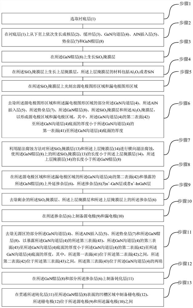
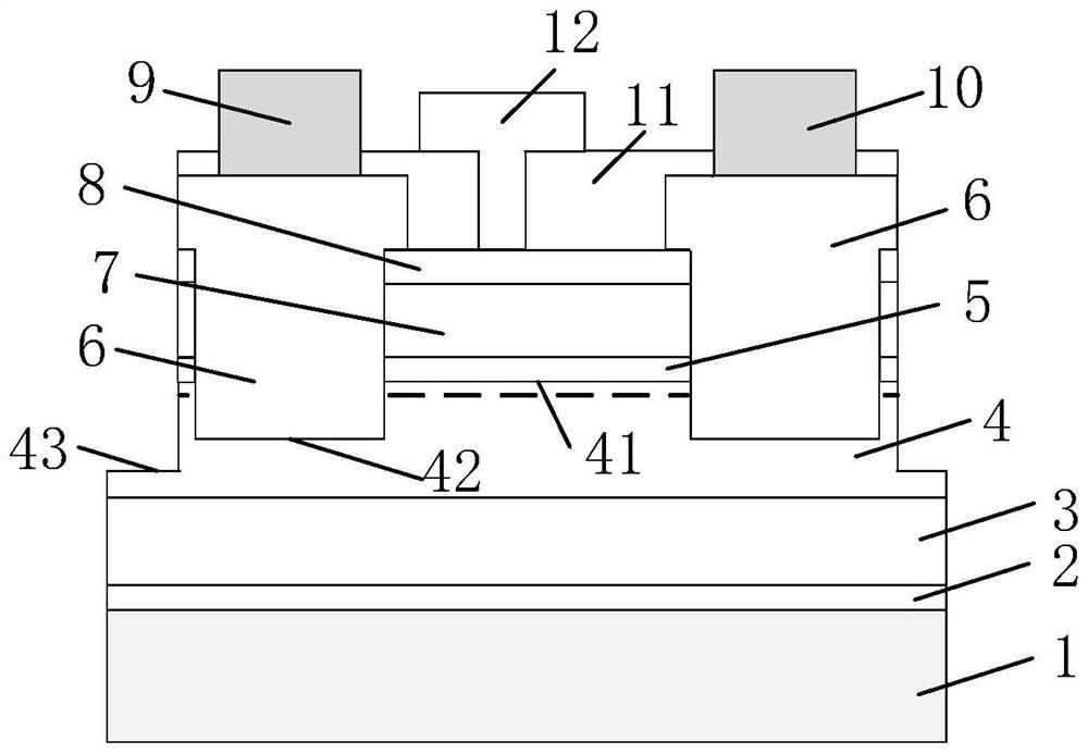
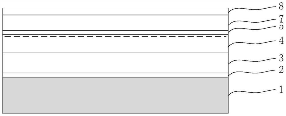
[0063] See figure 1 , figure 2 and Figure 3a-Figure 3i , figure 1 A schematic flow chart of a method for manufacturing a GaN-based HEMT device with high reliability and low contact resistance provided by an embodiment of the present invention, figure 2 A schematic structural diagram of a GaN-based HEMT device with high reliability and low contact resistance provided by an embodiment of the present invention, Figure 3a-Figure 3i It is a process schematic diagram of a method for preparing a low-resistance ohmic contact provided by an embodiment of the present invention. The invention provides a method for preparing a GaN-based HEMT device with high reliability and low contact resistance. The preparation method includes the following steps:
[0064] Step 1. Select the substrate layer 1.
[0065] Preferably, the material of the substrate layer 1 is SiC.
[0066] Step 2, see Figure 3a On the substrate layer 1, a nucleation layer 2, a buffer layer 3, a GaN channel layer ...
Embodiment 2
[0136] This embodiment provides a method for preparing a low contact resistance GaN-based device on the basis of the above-mentioned embodiments. The preparation method utilizes Al on the SiC substrate layer 1 2 o 3 / SiO 2 As an ohmic regrowth mask, a highly doped n + -GaN epitaxy to prepare low contact resistance GaN-based HEMT devices. The preparation method comprises the following steps:
[0137] Step 1. On the SiC substrate layer 1, use the MOCVD process to sequentially grow AlN nucleation layer 2, GaN buffer layer 3, GaN channel layer 4, AlN insertion layer 5, InAlN barrier layer 7, and GaN cap layer 8.
[0138] Step 2. Deposit SiO on the GaN cap layer 8 by PECVD 2 mask layer.
[0139] Specifically, using PECVD to deposit SiO on the sample 2 mask layer, using SiH 4 and N 2 O as a precursor to deposit SiO 2 , deposited with a thickness of 200nm, as the underlying regrowth mask layer.
[0140] Step 3, on SiO 2 Deposit Al on the mask layer by PEALD 2 o 3 mask la...
Embodiment 3
[0205] This embodiment provides a method for manufacturing a low contact resistance GaN-based device on the basis of the above embodiments. The method uses SiN / SiO on the SiC substrate layer 1 2 As an ohmic regrowth mask, highly doped n + -InGaN epitaxy to prepare low contact resistance GaN-based HEMT devices. The preparation method comprises the following steps:
[0206] Step 1. On the SiC substrate layer 1, use the MOCVD process to sequentially grow AlN nucleation layer 2, GaN buffer layer 3, GaN channel layer 4, AlN insertion layer 5, InAlN barrier layer 7, and GaN cap layer 8.
[0207] Step 2. Deposit SiO on the GaN cap layer 8 by PECVD 2 mask layer.
[0208] Specifically, using PECVD to deposit SiO on the sample 2 mask layer, using SiH 4 and N 2 O as a precursor to deposit SiO 2 , deposited with a thickness of 300nm as the underlying regrowth mask layer.
[0209] Step 3, on SiO 2 A SiN mask layer is deposited on the mask layer by PEALD.
[0210] Specifically, us...
PUM
 Abstract
Description
Claims
Application Information


