White light electroluminescent device and preparation method and application thereof

An electroluminescence device and electroluminescence technology, which are applied in the fields of electro-solid devices, semiconductor/solid-state device manufacturing, electrical components, etc., can solve the problem of poor electroluminescence spectral stability, poor charge transfer and injection performance, and difficulty in meeting high-quality lighting. and other issues, to achieve high external quantum efficiency, reduce material costs, and achieve the effect of external quantum efficiency

Pending Publication Date: 2022-04-22
SOUTH CHINA UNIV OF TECH
View PDF0 Cites 0 Cited by
  • Summary
  • Abstract
  • Description
  • Claims
  • Application Information

AI Technical Summary

Problems solved by technology

However, the application of this class of materials in white light electroluminescent devices is limited due to poor charge transport and injection properties.
Although the use of rare metal-doped or heterogeneous perovskites to fabricate single-emitting layer white electroluminescent devices has been reported, and the highest external quantum efficiency can reach 6.5%, but the electroluminescence spectra of them under different driving voltages are different. Poor stability, difficult to meet the requirements of high-quality lighting
In addition, although some perovskites with high photoluminescence efficiency and complementary color organic polymers or oligomers can be simply mixed to form a single-layer white light-emitting device, the energy transfer will decrease with the decrease of the distance between molecules. Small but increasing, it will cause quenching of blue light emission, and the maximum external quantum efficiency of the final device is less than 0.1%
In addition, some double-layer or tandem structures have been proven to effectively suppress the energy transfer process, and the maximum external quantum efficiency of the device can reach 1.3%, but the fine device structure and complex process will lead to a substantial increase in the production cost of the device, and the application is limited. very restrictive

Method used


Image

  • White light electroluminescent device and preparation method and application thereof
  • White light electroluminescent device and preparation method and application thereof
  • White light electroluminescent device and preparation method and application thereof

Examples


Embodiment 1

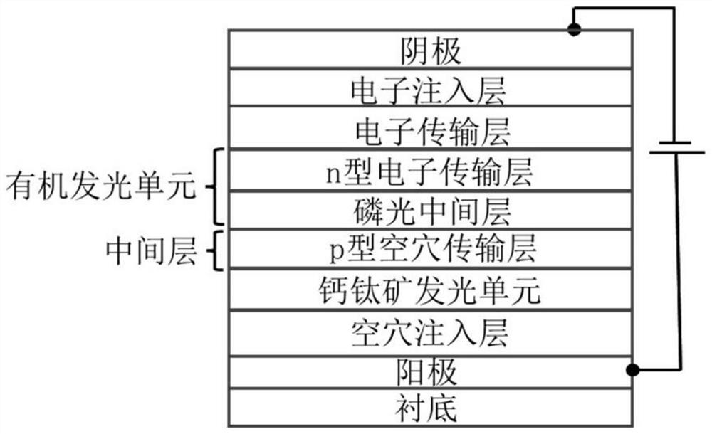
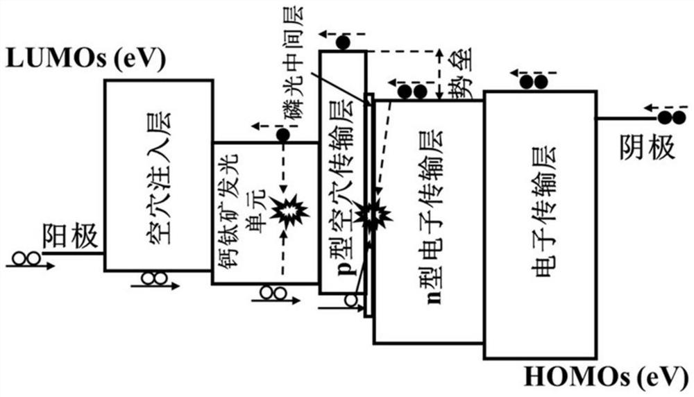
[0045] A kind of white electroluminescent device (structural schematic diagram is as figure 1 As shown, the schematic diagram of the distribution of energy levels and exciton recombination regions is shown in figure 2 shown), which consists of a substrate (ITO glass substrate), a hole injection layer (m-PEDOT:PSS with a thickness of 30nm), a perovskite light-emitting unit, a p-type hole transport layer (intermediate layer; a thickness of 5nm TAPC), phosphorescent interlayer (FIrpic with 1nm thickness), n-type electron transport layer (BOCzPh with 20nm thickness), electron transport layer (TPBi with 30nm thickness), electron injection layer (CsF ) and cathode (Al with a thickness of 120nm), where the ITO glass substrate is both the substrate and the anode, m-PEDOT:PSS is the hole injection layer, TPBi is the electron transport layer, and CsF is the electron injection layer , the perovskite light-emitting unit, the intermediate layer and the organic light-emitting unit (TAPC / F...

Embodiment 2

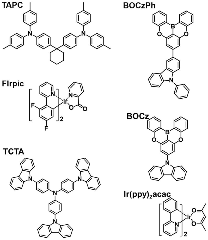
[0060] A kind of white light electroluminescent device, it is by ITO glass substrate, thickness is the m-PEDOT:PSS of 30nm, perovskite light-emitting unit, thickness is the TCTA of 5nm:Ir(ppy) 2 acac (3wt%), TAPC:BOCz (1:1):FIrpic (10wt%) with a thickness of 20nm, TPBi with a thickness of 30nm, CsF with a thickness of 1.2nm and Al with a thickness of 120nm. The ITO glass substrate is both the substrate and the anode, m-PEDOT:PSS is the hole injection layer, TPBi is the electron transport layer, CsF is the electron injection layer, the perovskite light-emitting unit and the intermediate layer (TCTA:Ir(ppy)2acac ) and the organic light-emitting unit (TAPC:BOCz:FIrpic) are the common light-emitting layer (the structural formula of the light-emitting material in the organic light-emitting unit is as follows image 3 shown).

[0061] The preparation method of the above-mentioned white light electroluminescence device comprises the following steps:

[0062] 1) Clean the ITO glass ...


PUM

PropertyMeasurementUnit
thicknessaaaaaaaaaa
thicknessaaaaaaaaaa
thicknessaaaaaaaaaa

Abstract

The invention discloses a white light electroluminescent device and a preparation method and application thereof. The white light electroluminescent device comprises a laminated structure formed by a perovskite light-emitting unit, a middle layer and an organic light-emitting unit in sequence, spectrums of the perovskite light-emitting unit and the organic light-emitting unit are complementary, and the two light-emitting units jointly emit and are compounded to obtain white light. The preparation method of the white light electroluminescent device comprises the following steps: sequentially depositing each layer in a spin coating, spray coating, blade coating, thermal evaporation, printing or ink-jet printing manner to form a laminated structure, thereby obtaining the white light electroluminescent device. The white light electroluminescent device has the advantages of high efficiency, stable spectrum and the like, is low in manufacturing cost and simple in preparation process, and can completely meet the requirements of high-quality illumination and display.

Description

technical field [0001] The invention relates to the technical field of light emitting devices, in particular to a white light electroluminescent device and its preparation method and application. Background technique [0002] Organometallic halide perovskite materials are an important optoelectronic material with the general structural formula ABX 3 , where A represents the organic monovalent cation CH 3 NH 3 + (MA + ), CH(NH 2 ) 2 + (FA + ) or inorganic monovalent cation Cs + , B represents the metal ion Pb 2+ or Sn 2+ , X stands for Cl - 、Br - or I - . Organometal halide perovskite materials have the advantages of high carrier mobility, high photoluminescence efficiency, high color purity, adjustable band gap, and low cost, and have great application potential in the fields of lighting and display. [0003] In recent years, the external quantum efficiency of perovskite-based green, red, and near-infrared electroluminescent devices has exceeded 20%, while the...

Claims


Application Information

Patent Timeline
Patent Type & Authority Applications(China)
IPC IPC(8): H01L51/50H01L51/56
CPCH10K50/13H10K71/00
Inventor 苏仕健刘邓辉刘鑫妍甘亦阳
Owner SOUTH CHINA UNIV OF TECH
Why Eureka
Try Eureka