
Semiconductor structure and manufacturing method thereof

A manufacturing method and semiconductor technology, applied in semiconductor/solid-state device manufacturing, semiconductor devices, electrical components, etc., can solve the problems of bottom ion implantation angle limitation, complicated process steps, high process cost, etc., so as to save production time and reduce costs , The effect of simplifying the process steps

Pending Publication Date: 2022-04-29
SHANGHAI INTEGRATED CIRCUIT EQUIP & MATERIALS IND INNOVATION CENT CO +1
View PDF0 Cites 2 Cited by
  • Summary
  • Abstract
  • Description
  • Claims
  • Application Information

AI Technical Summary

Problems solved by technology

[0006] Repeated use of photolithography, etching, ion implantation, and cleaning steps increases the probability of defects, and also takes into account the pattern differences caused by multiple exposures, and the process steps are more complicated and the corresponding process costs are relatively high.
At the same time, due to the accumulation of etching products during the etching process, the angle of ion implantation at the bottom is limited, and the process window is low.

Method used


Image

  • Semiconductor structure and manufacturing method thereof
  • Semiconductor structure and manufacturing method thereof
  • Semiconductor structure and manufacturing method thereof

Examples


Embodiment Construction

[0041] In order to make the purpose, advantages and features of the present invention clearer, the present invention will be further described in detail below in conjunction with the accompanying drawings and specific embodiments. It should be noted that the drawings are all in very simplified form and not drawn to scale, and are only used to facilitate and clearly assist the purpose of illustrating the embodiments of the present invention. In addition, the structures shown in the drawings are often a part of the actual structure. In particular, each drawing needs to display different emphases, and sometimes uses different scales.

[0042]As used in the present invention, the singular forms "a", "an" and "the" include plural objects, the term "or" is usually used in the sense of including "and / or", and the term "several" Usually, the term "at least one" is used in the meaning of "at least one", and the term "at least two" is usually used in the meaning of "two or more". In ad...


PUM


Abstract

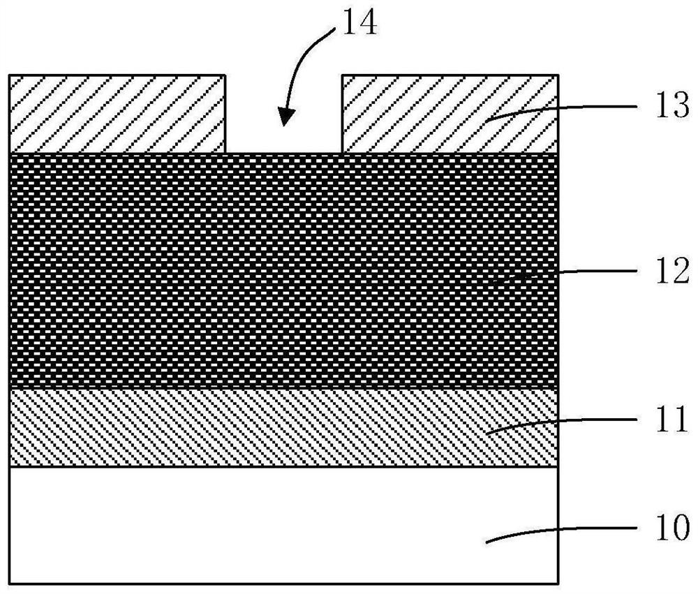
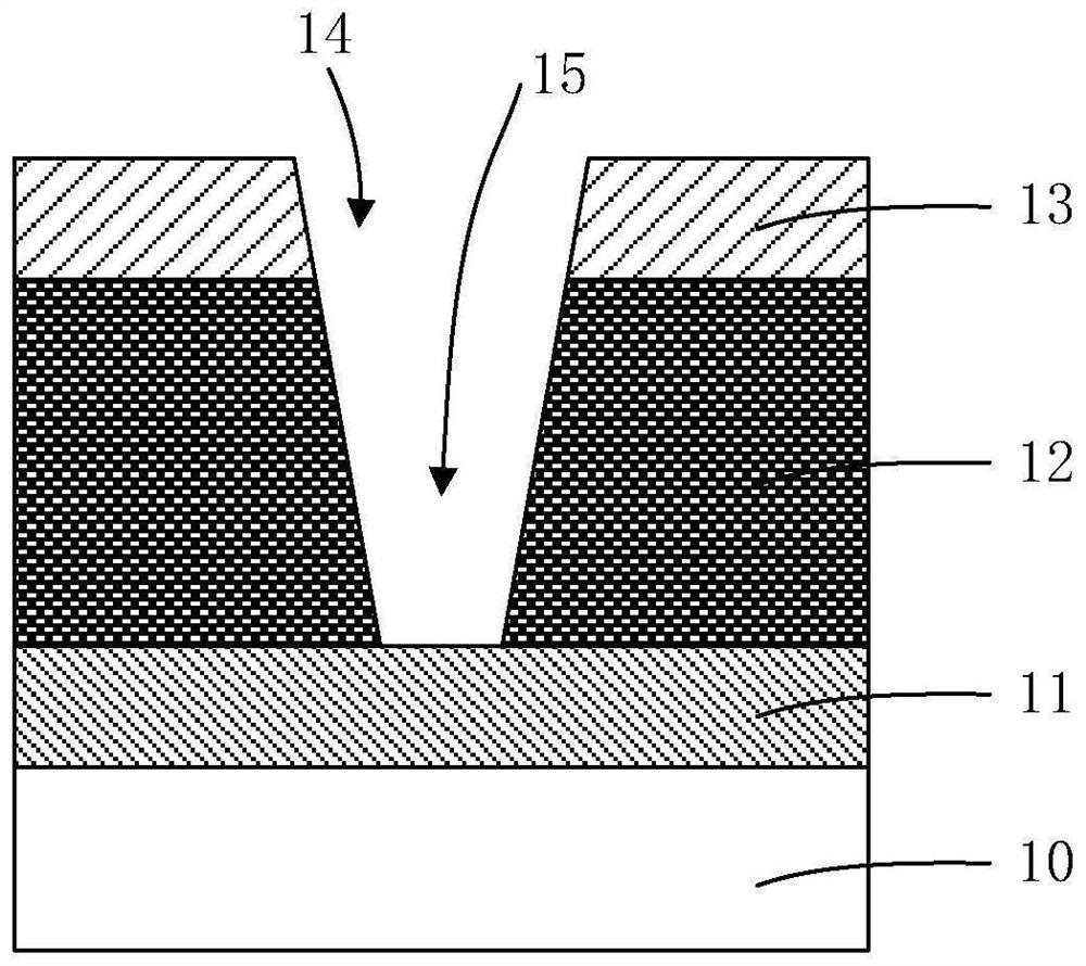
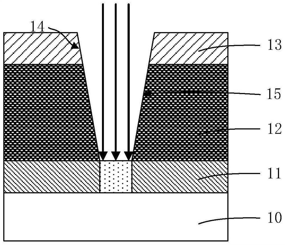
The invention provides a semiconductor structure and a manufacturing method thereof, and the method comprises the steps: providing a substrate, and sequentially forming a pattern definition layer, a pattern transfer layer and a pattern mask layer on the substrate; etching the pattern mask layer to form a first groove exposing the pattern transfer layer; the pattern transfer layer at the bottom of the first groove is etched, a second groove exposing the pattern definition layer is formed, and the side wall of the second groove is perpendicular to the upper surface of the pattern definition layer; and carrying out ion doping on the exposed pattern definition layer through the first groove and the second groove, wherein the pattern definition layer doped with ions is used as a metal blocking layer. Compared with the prior art, the metal blocking layer with the same size can be finally formed by forming the first groove with the small opening size, so that the adjacent metal blocking layers can be formed in the same process step, the process steps are simplified, the manufacturing time is saved, the occurrence rate of process defects is reduced, and the cost is reduced.

Description

technical field [0001] The invention relates to the technical field of integrated circuit manufacturing, in particular to a semiconductor structure and a manufacturing method thereof. Background technique [0002] With the continuous improvement of the integration level of integrated circuits, the chip size is getting smaller and smaller. Limited by the limit of deep ultraviolet lithography (DUV), it is impossible to directly form metal interconnection patterns through lithography. A common technique for resistive isolation. [0003] The Metal Cut (metal blocking) manufacturing process is formed in the semiconductor metal interconnection blocking area, and uses inorganic materials (generally amorphous silicon) to isolate the metal interconnection pattern. Because the size of the metal interconnect isolation structure shrinks, more and more photomasks are required as the process node progresses. The existing process is to form a pattern by photolithography, then etch a patt...

Claims


Application Information

Patent Timeline
Patent Type & Authority Applications(China)
IPC IPC(8): H01L21/76H01L29/06
CPCH01L21/76H01L29/0642
Inventor 王兆龙
Owner SHANGHAI INTEGRATED CIRCUIT EQUIP & MATERIALS IND INNOVATION CENT CO
Learn More