Eureka AIR delivers breakthrough ideas for toughest innovation challenges, trusted by R&D personnel around the world.

Hydrogen absorption device for hydrogen sensitive hybrid integrated circuit and preparation method thereof

A hybrid integrated circuit, sensitive technology, applied in the direction of electric solid-state devices, circuits, electrical components, etc., can solve the problems of poor robustness, high cost, low hydrogen absorption efficiency/rate, etc.

Active Publication Date: 2022-05-20
南京盖特尔电子科技有限公司
View PDF7 Cites 1 Cited by
  • Summary
  • Abstract
  • Description
  • Claims
  • Application Information

AI Technical Summary

Problems solved by technology

[0005] At present, the method of hydrogen-absorbing components used in hydrogen-sensitive hybrid integrated circuits is mainly to use titanium metal sheet as the hydrogen-absorbing material, and then electroplate or magnetron sputtering on its surface to coat hundreds of nanometers of palladium metal as a protective layer, or magnetic Controlled sputtering titanium / palladium metal is used as transition layer and protective layer respectively, as disclosed in Chinese patent application CN110863174A a kind of titanium-based hydrogen-absorbing material that does not need activation and its preparation method and a kind of hydrogen-absorbing material that is used for electronic packaging disclosed in CN110699649 and its preparation method, although the hydrogen absorbing device of this structure is effective, the hydrogen absorbing efficiency / rate is relatively low, and the use robustness is not good, and the Ti substrate and the Pd film combined with the catalytic cracking and permeation effect on the Ti substrate, Although the performance of the product using palladium metal is good, in order to obtain a better hydrogen absorption effect, it needs to be thicker, resulting in high cost

Method used


Image

  • Hydrogen absorption device for hydrogen sensitive hybrid integrated circuit and preparation method thereof
  • Hydrogen absorption device for hydrogen sensitive hybrid integrated circuit and preparation method thereof
  • Hydrogen absorption device for hydrogen sensitive hybrid integrated circuit and preparation method thereof

Examples


Embodiment 1

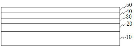
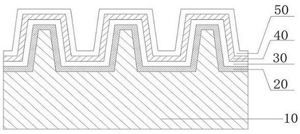
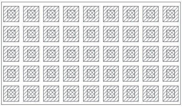
[0131]With a 0.3mm thick alumina ceramic sheet as a carrier, a cuboid micro-cone with a height of 0.8mm×0.8mm×0.1mm (length×width×height) and an inclination angle of 80 degrees is formed on the surface to enhance the specific surface, and the entire surface passes through Chemical roughening further enhances the specific surface, such as Figure 3a shown. Then prepare the surface film layer by magnetron sputtering process, cover the surface of the carrier with 20 μm 4N (purity 99.99%) metal titanium as the hydrogen absorption layer, and cover the hydrogen absorption layer with 1 μm thick cobalt as the selective hydrogen permeation layer. Cover the selective hydrogen permeation layer with palladium with a thickness of 10nm as a protective layer, and finally, spray a layer of PDMS with a thickness of 10 μm on the surface as an anti-particle shedding layer, such as Figure 3b shown.

[0132] in Figure 3b It shows the schematic structure of the surface film layer prepared on t...

Embodiment 2

[0134] A 10mm×5mm×1mm (length×width×height) zero-order sponge titanium is used as a carrier and a hydrogen absorbing layer, and a layer of 500nm thick metal palladium is electroplated on its surface and hole wall as a selective hydrogen permeating layer and a protective layer ,Such as Figure 4a As shown; then the surface is sprayed with a layer of 15 μm polystyrene (Polystyrene: MW=280K) polymer film as an anti-particle shedding layer. In this embodiment, the same metal palladium is used for the selective hydrogen permeable layer and the protective layer. Do.

[0135] in, Figure 4b Indicates that the zero-grade sponge titanium includes: 500nm-thick metal palladium doubles as a selective hydrogen permeation layer and a protective layer, and a 15μm-thick polystyrene (Polystyrene: MW=280K) polymer film anti-particle shedding layer.

Embodiment 3

[0137] 3N5 (purity 99.95%) titanium belt (thickness 0.2mm) is used as the carrier and hydrogen absorbing layer, and the surface is enhanced by surface enhancement processing to form micro-cone grooves with a height of about 50 microns to enhance the specific surface, such as Figure 5a As shown; Cobalt with a thickness of 0.5 μm is used as a selective hydrogen permeation layer and palladium with a thickness of 10 nm is used as a protective layer, and no anti-particle shedding layer is used.

[0138] Figure 5b It shows the schematic structure of the surface film layer prepared on the basis of the titanium tape carrier, including a cobalt selective hydrogen permeation layer with a thickness of 0.5 μm and a palladium protective layer with a thickness of 10 nm.

[0139] Wherein, numeral 12 represents a micro-cone groove structure.


PUM

PropertyMeasurementUnit
thicknessaaaaaaaaaa
thicknessaaaaaaaaaa
thicknessaaaaaaaaaa

Abstract

The invention relates to the field of integrated circuits, and provides a hydrogen absorption device for a hydrogen-sensitive hybrid integrated circuit. The hydrogen absorption layer, the selective hydrogen permeation layer and the protective layer are sequentially stacked on the surface of the carrier; wherein the hydrogen absorption layer covers the surface of the carrier and is used for absorbing / storing hydrogen; the selective hydrogen permeation layer covers the hydrogen absorption layer and is used for selectively allowing hydrogen to permeate and preventing other gases from permeating; and the protective layer adopts a metal / alloy film with stable properties in an air environment, covers the selective hydrogen permeation layer in a covering manner, and is used for allowing hydrogen to permeate and protecting the selective hydrogen permeation layer below the protective layer from reacting with gas in air to weaken hydrogen permeation.

Description

technical field [0001] The invention relates to the field of hybrid integrated circuits, in particular to a selective hydrogen absorbing device in a hybrid integrated circuit package, in particular to a hydrogen absorbing device for a hydrogen-sensitive hybrid integrated circuit, which is suitable for packaging a hydrogen-sensitive hybrid integrated circuit Selective absorption of hydrogen in order to improve the reliability and lifetime of hybrid IC packages. Background technique [0002] Since various active devices (such as various semiconductor chips) and passive devices (such as packaging substrates, packaging shells, wave-absorbing plates, etc.) , eutectic, gluing, etc.) will inevitably introduce hydrogen, or the chemical reaction in the manufacturing process and packaging process will produce hydrogen. The hydrogen will be absorbed by active devices, passive devices, and packaging modules (such as some metals, alloys, composite materials, organic materials, etc.) wit...

Claims


Application Information

Patent Timeline
Patent Type & Authority Applications(China)
IPC IPC(8): H01L23/26C23C14/35C23C14/14C25D7/00
CPCH01L23/26C23C14/35C23C14/14C25D7/00Y02E60/32
Inventor 王列松黄寇华
Owner 南京盖特尔电子科技有限公司
Why Eureka
Eureka Blog
Learn More