Preparation method of semiconductor device

A semiconductor and device technology, which is applied in the field of semiconductor device preparation, can solve the problems of increasing on-resistance, increasing device size, and low doping concentration, and achieves the effect of improving electrical performance, reducing possibility, and not increasing electric field intensity

Active Publication Date: 2022-08-02
GUANGZHOU CANSEMI TECH INC
View PDF6 Cites 0 Cited by
  • Summary
  • Abstract
  • Description
  • Claims
  • Application Information

AI Technical Summary

Problems solved by technology

[0002] Among power field effect transistors, the most important one is a lateral double-diffused metal-oxide field effect transistor (LDMOS). In the design process of LDMOS devices, the optimization of the surface lateral voltage region is very important, which is directly related to the performance of the device. Advantages and disadvantages, LDMOS devices should have a lateral withstand voltage region with sufficient length and low doping concentration to obtain the required high breakdown voltage, but it will increase the device size and increase the on-resistance when conducting current

Method used


Image

  • Preparation method of semiconductor device
  • Preparation method of semiconductor device
  • Preparation method of semiconductor device

Examples


preparation example Construction

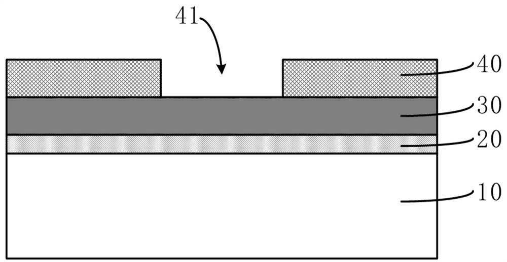
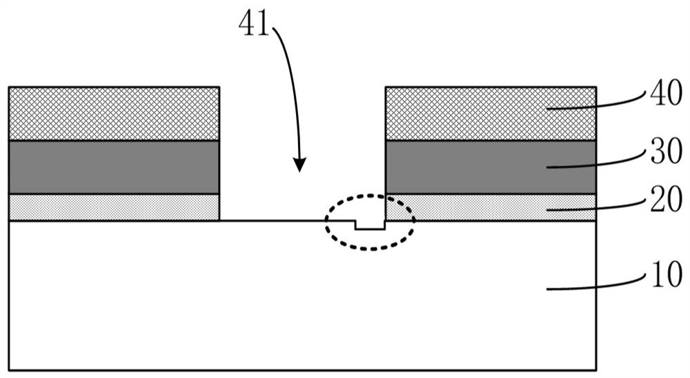
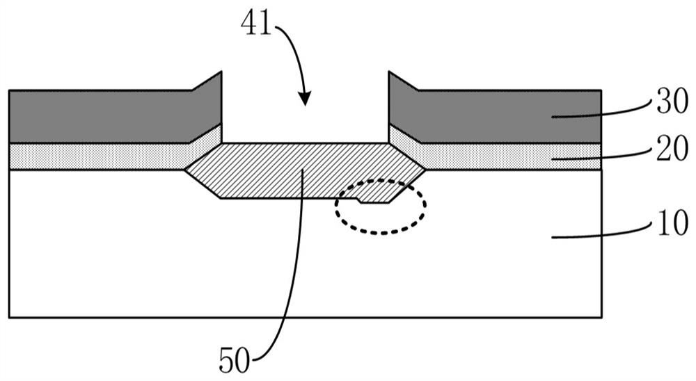
[0024] Figure 1A~1C It is a schematic cross-sectional view of the corresponding steps in the preparation method of a semiconductor device, which is combined below Figure 1A~1C The preparation method of the semiconductor device is described in detail, and the semiconductor device is an LDMOS device.

[0025] Please refer to Figure 1A , a substrate 10 is provided, a first dielectric layer 20, a second dielectric layer 30 and a patterned photoresist layer 40 are sequentially formed on the substrate 10, the patterned photoresist layer 40 has an opening 41, and the opening 41 exposes On the surface of the second dielectric layer 30 , the material of the first dielectric layer 20 may be oxide, and the material of the second dielectric layer 30 may be nitride.

[0026] Please refer to Figure 1B , using a dry etching process to etch the first dielectric layer 20 and the second dielectric layer 30 downward along the opening 41 to expose the surface of the substrate 10, and the ope...


PUM

PropertyMeasurementUnit
thicknessaaaaaaaaaa
thicknessaaaaaaaaaa
thicknessaaaaaaaaaa

Abstract

The present invention provides a method for preparing a semiconductor device, comprising: providing a substrate, on which a first dielectric layer, a second dielectric layer and a patterned photoresist layer are sequentially formed, and the patterned photoresist layer is formed in sequence on the substrate. The resist layer has an opening; a dry etching process is used to etch the second dielectric layer along the opening to reveal the surface of the first dielectric layer, and the opening extends to the surface of the first dielectric layer surface; continuing to etch the first dielectric layer along the opening by a wet etching process to reveal the surface of the substrate, and the opening extends to the surface of the substrate; and, removing the patterning A field oxide layer is formed on the surface of the substrate at the bottom of the opening; the invention improves the smoothness of the interface between the field oxide layer and the substrate, improves the avalanche resistance of the device, thereby improving the the electrical properties of semiconductor devices.

Description

technical field [0001] The present invention relates to the technical field of semiconductors, and in particular, to a method for preparing a semiconductor device. Background technique [0002] Among the power field effect transistors, the more important one is a lateral double-diffused metal-oxide field effect transistor (LDMOS). In the design process of LDMOS devices, the optimization of the surface lateral voltage region is very important, which is directly related to the performance of the device. Advantages and disadvantages, the LDMOS device should have a lateral withstand voltage region with a long enough length and low doping concentration to obtain the required high breakdown voltage, but it will increase the size of the device and increase the on-resistance when conducting current. One of the keys to optimizing the lateral withstand voltage region of the surface is to suppress the curvature effect of the PN junction. In actual power semiconductor devices, not all P...

Claims


Application Information

Patent Timeline
Patent Type & Authority Patents(China)
IPC IPC(8): H01L21/02B08B3/08
CPCH01L21/02057H01L21/02052B08B3/08
Inventor 李超成
Owner GUANGZHOU CANSEMI TECH INC
Why Eureka
Try Eureka