Heterojunction solar cell and preparation method thereof

A solar cell and heterojunction technology, applied in circuits, electrical components, photovoltaic power generation, etc., can solve problems such as increased photon absorption rate, efficiency loss, and photon reduction, so as to enhance light trapping, improve conversion efficiency, and promote absorption The effect of using

Inactive Publication Date: 2022-06-03
晋能光伏技术有限责任公司 +1
View PDF8 Cites 2 Cited by
  • Summary
  • Abstract
  • Description
  • Claims
  • Application Information

AI Technical Summary

Problems solved by technology

The efficiency loss mainly comes from the thermalization loss of photons with energy higher than the bandgap, and the loss that photons with energy lower than the bandgap cannot be absorbed and utilized
Among them, some ultraviolet short-wave photons carry energy higher than the forbidden band width of silicon solar cells, and the excess energy will be lost in the form of heat, which not only causes short-wave photon energy loss, but also generates heat. The output power adversely affects the
This short-wavelength photon loss effect is particularly evident in heterojunction cell structures, because the amorphous silicon film layer in the standard heterojunction cell structure is thicker than the conventional diffusion layer, doped amorphous silicon layer and intrinsic amorphous The thickness of the silicon layer is about 8-15nm, which leads to an increase in the photon absorption rate of the amorphous silicon film layer in the short-wave region, thereby reducing the photons reaching the substrate, further reducing the effective utilization of photons, and affecting the final conversion efficiency of the battery.

Method used


Image

  • Heterojunction solar cell and preparation method thereof
  • Heterojunction solar cell and preparation method thereof
  • Heterojunction solar cell and preparation method thereof

Examples


Embodiment Construction

[0020] The specific embodiments of the present invention will be described in further detail below with reference to the accompanying drawings and embodiments. The following examples are intended to illustrate the present invention, but not to limit the scope of the present invention.

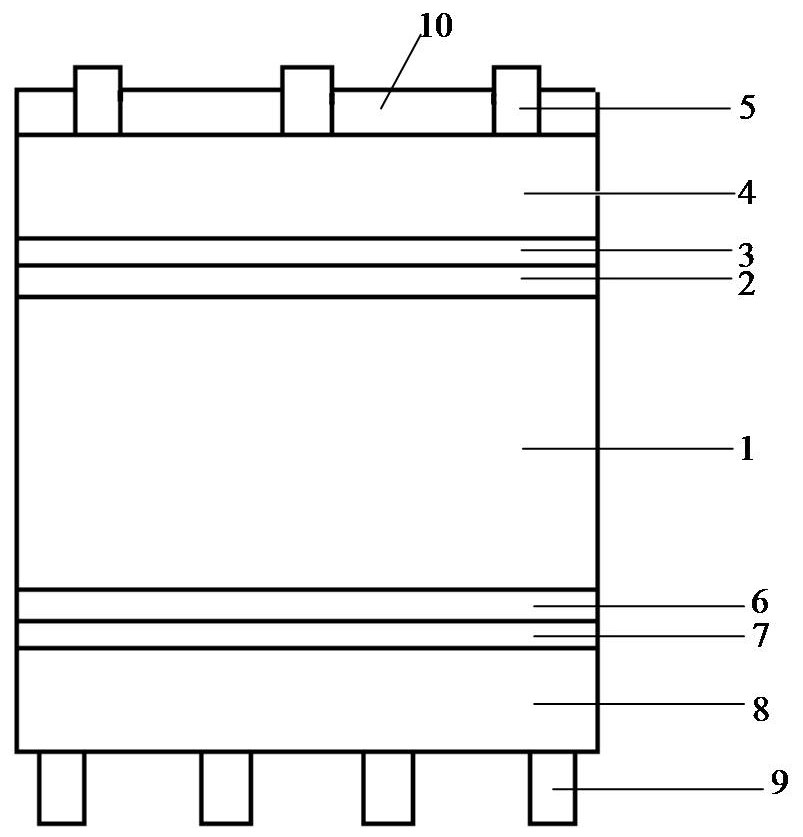
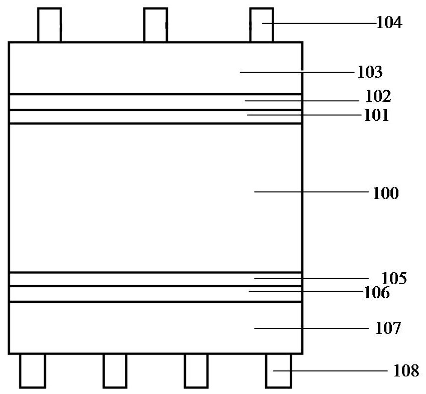
[0021] like figure 1 As shown, the heterojunction solar cell provided by the present invention includes a crystalline silicon substrate 1, and the front surface of the crystalline silicon substrate 1 is sequentially deposited with a front intrinsic amorphous silicon layer 2, an N-type doped layer 3, and a front TCO layer. layer 4 and front metal electrode 5; the back surface of the crystalline silicon substrate 1 is sequentially deposited with a back intrinsic amorphous silicon layer 6, a P-type doped layer 7, a back TCO layer 8 and a back metal electrode 9. The front metal electrode The thin grid electrode in 5 and the front TCO layer 4 not shielded by the metal electrode are covered with a f...


PUM

PropertyMeasurementUnit
thicknessaaaaaaaaaa
thicknessaaaaaaaaaa
thicknessaaaaaaaaaa

Abstract

The invention relates to a heterojunction solar cell and a preparation method thereof, and belongs to the technical field of solar cell manufacturing. Comprising a crystalline silicon substrate, and a front intrinsic amorphous silicon layer, an N-type doped layer, a front TCO layer and a front metal electrode are sequentially deposited on the front surface of the crystalline silicon substrate; a back intrinsic amorphous silicon layer, a P-type doped layer, a back TCO layer and a back metal electrode are sequentially deposited on the back of the crystalline silicon substrate, and a functional film containing a down-conversion fluorescent material covers a fine gate electrode in the front metal electrode and the front TCO layer which is not shielded by the metal electrode. By introducing the functional film containing the down-conversion fluorescent material, photons in a short-wave region which cannot be utilized by a solar cell can be converted into photon energy matched with spectral response of the photons, namely photons below 400nm are absorbed and converted into low-energy photons of 400-1100nm, so that absorption and utilization of the cell to sunlight are promoted, and the conversion efficiency of the solar cell is improved. The conversion efficiency of the heterojunction solar cell is improved, and the damage effect of part of ultraviolet light on the cell is weakened.

Description

technical field [0001] The invention relates to the technical field of solar cell manufacturing, in particular to a heterojunction solar cell and a preparation method thereof. Background technique [0002] With the increasing demand for energy in the world and the aggravation of carbon emissions, the development of a clean energy system is imminent. As the most potential new energy technology, solar cell technology has been widely studied in recent years. Among them, silicon-based solar cells dominate the application scale and industrial mass production of the photovoltaic industry due to their efficiency advantages. After PERC (back passivation contact cell) battery technology, HJT (silicon-based heterojunction cell), TopCON (tunnel oxide passivation contact), IBC (interdigital back contact cell) are considered to be the most potential at present. three high-efficiency battery technologies. As of March 2022, among all battery technologies that have issued efficiency cert...

Claims


Application Information

Patent Timeline
Patent Type & Authority Applications(China)
IPC IPC(8): H01L31/0216H01L31/055H01L31/0747H01L31/20
CPCH01L31/0747H01L31/202H01L31/055H01L31/02168Y02E10/50
Inventor 鲍少娟王继磊杨立友黄金白焱辉任法渊杨骥杨文亮
Owner 晋能光伏技术有限责任公司
Why Eureka
Try Eureka