Double-layer waveguide three-dimensional stacked low-voltage miniature silicon-based optical modulator

A stacked, double-layer technology, applied in the direction of instruments, optics, nonlinear optics, etc., to achieve low-voltage drive, reduce drive voltage, and reduce area

Pending Publication Date: 2022-06-10
GUILIN UNIV OF ELECTRONIC TECH
View PDF0 Cites 0 Cited by
  • Summary
  • Abstract
  • Description
  • Claims
  • Application Information

AI Technical Summary

Problems solved by technology

Since the two waveguide structures in the modulation unit of this type of modulator are built on a silicon substrate, the longer modulation unit structure occupies a larger area, which is not conducive to the integration of optical devices.

Method used


Image

  • Double-layer waveguide three-dimensional stacked low-voltage miniature silicon-based optical modulator
  • Double-layer waveguide three-dimensional stacked low-voltage miniature silicon-based optical modulator
  • Double-layer waveguide three-dimensional stacked low-voltage miniature silicon-based optical modulator

Examples


Embodiment Construction

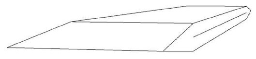
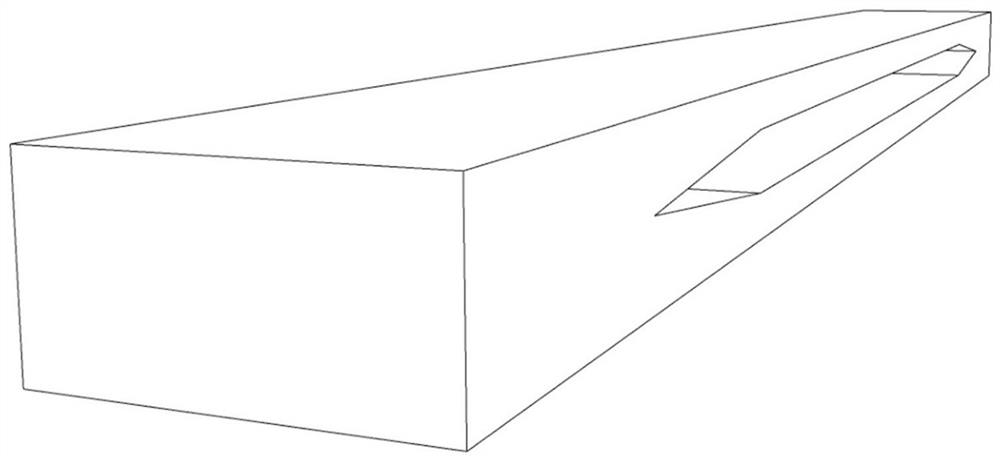
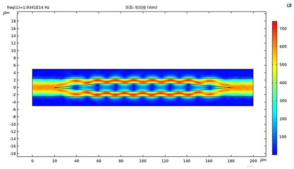
[0036] The working temperature of this example is 293.15K, the incident light wavelength is 1.55um, the refractive index of the cladding layer is 1.53, and the refractive index of the core layer is 2.22. The total length of the modulator is 200um, the width is 40um, and the height is 10um. Figure 7The silicon dioxide film 2-3 shown has a total length of 140um, a height of 2um, and a width of 20um. Among them, the base of the beam-splitting isosceles triangle and the interference isosceles triangle is 2um, and the height is 40um. Figure 8 The shown optical waveguide structure has a length of 140um, a width of 20um, and a height of 7um.

[0037] Use the "Electromagnetic Waves, Frequency Domain (ewfd)" interface in the COMSOL Wave Optics Module and the "Electrostatics (es)" interface in the AC / DC Module for simulation. In order to improve the simulation efficiency, a two-dimensional space is firstly used for modeling.

[0038] Draw in COMSOL "Geometry" such as image 3 The ...


PUM

PropertyMeasurementUnit
lengthaaaaaaaaaa
refractive indexaaaaaaaaaa

Abstract

The invention relates to a double-layer waveguide three-dimensional stacked low-voltage miniature silicon-based optical modulator based on a Mach-Zehnder interference principle. The stacked Mach-Zehnder modulator is specifically composed of three parts: an optical coupling unit composed of a square waveguide and used for transmitting light waves to a designed stacked Mach-Zehnder modulation unit; the stacked Mach-Zehnder modulation unit is used for modulating the light wave; and the light wave interference unit is used for coupling the two modulated light waves to generate an interference phenomenon. Wherein the stacked Mach-Zehnder modulation unit is composed of double-layer waveguides, the occupied area of the device is reduced, the double-layer waveguides are covered by metal films, and an electric field of the metal films is controlled under the action of external programmable low-voltage signals, so that the refractive indexes of the two waveguides of the modulation unit are changed, and a phase difference is generated between output light waves of the two waveguides; and finally, the light wave modulation function is realized. Through input of given voltage codes, rapid switching of two phase differences can be realized, and the function of the optical switch can be realized under specific voltage modulation. The method can be widely applied to design of silicon-based optical integrated circuits and electro-optical chips.

Description

technical field [0001] The invention relates to the field of silicon-based photonic chip integrated devices, in particular to a double-layer waveguide three-dimensional stacked low-voltage micro-silicon-based optical modulator based on the Mach-Zehnder interference principle. Background technique [0002] Optical modulation technology is a modulation technology that superimposes a signal carrying information on the carrier light wave. Optical modulation can make certain parameters of light waves, such as amplitude, frequency, phase, polarization state and duration, change according to certain rules. A device that realizes light modulation is called a light modulator. [0003] An optical switch is a specific optical modulation device that can convert optical signals in optical transmission lines or integrated optical circuits into logic signals. [0004] Mach-Zehnder interference divides a beam of light into two beams of equal power, and by changing the relative speed or op...

Claims


Application Information

Patent Timeline
Patent Type & Authority Applications(China)
IPC IPC(8): G02F1/035G02F1/03G02F1/01
CPCG02F1/035G02F1/0316G02F1/0113G02F1/0102
Inventor 许川佩展翔马贤唐鹏牛军浩胡聪陈涛
Owner GUILIN UNIV OF ELECTRONIC TECH
Why Eureka
Try Eureka