Manufacturing method of semiconductor structure and semiconductor structure

A manufacturing method and semiconductor technology, applied in semiconductor/solid-state device manufacturing, semiconductor devices, transistors, etc., can solve problems affecting the performance of transistors and access performance of DRAM devices, so as to improve switching speed, reduce quantum tunneling effect, The effect of improving stability

Pending Publication Date: 2022-07-19
CHANGXIN MEMORY TECH INC
View PDF0 Cites 0 Cited by
  • Summary
  • Abstract
  • Description
  • Claims
  • Application Information

AI Technical Summary

Problems solved by technology

[0004] However, the high thermal budget during the forming process of the amorphous silicon layer of the furnace tube will affect the work function adjustment process of the work function layer to the transistor, affect the performance of the transistor, and thus affect the access performance of the DRAM device

Method used


Image

  • Manufacturing method of semiconductor structure and semiconductor structure
  • Manufacturing method of semiconductor structure and semiconductor structure
  • Manufacturing method of semiconductor structure and semiconductor structure

Examples


Embodiment Construction

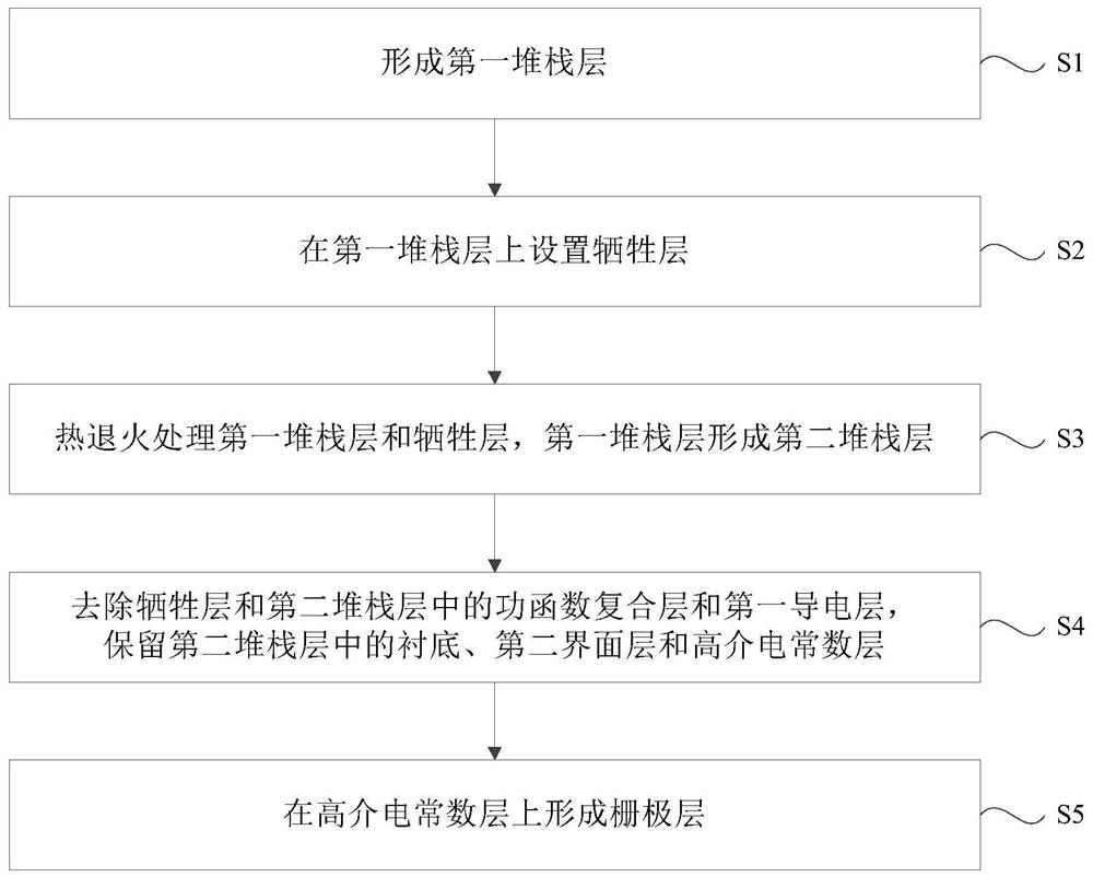
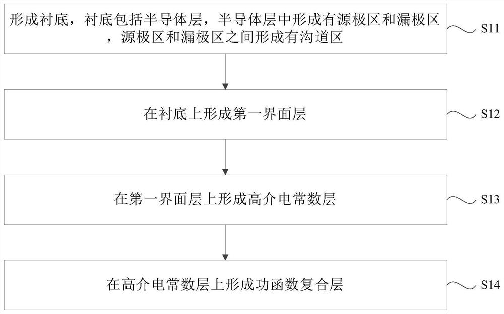
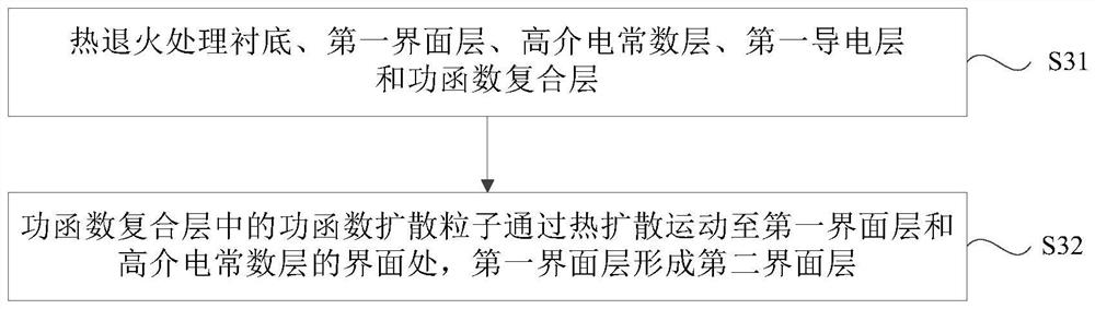
[0078] During the actual research process, the inventors of the present application found that when using HKMG technology to manufacture transistors, the heat treatment process and heat treatment annealing process are generally completed in a heat treatment furnace. An amorphous silicon layer is formed on the surface of the layer, and finally a metal gate is formed. Since the polysilicon sacrificial layer grown through the furnace tube requires a long-term high-temperature growth process, this process will generate a large thermal budget, resulting in a decrease in the amount of heat reserved for the work function adjustment process, resulting in the work function adjustment process. , the work function diffusion particles cannot obtain enough energy to diffuse to the predetermined layer position, so that the work function adjustment process cannot be completed. Moreover, in the process of growing the polysilicon sacrificial layer in the furnace tube, the high temperature proc...


PUM

PropertyMeasurementUnit
thicknessaaaaaaaaaa

Abstract

The invention provides a manufacturing method of a semiconductor structure and the semiconductor structure, relates to the technical field of semiconductor manufacturing, and aims to solve the problems that the thermal budget is relatively high in the manufacturing process of an existing semiconductor structure, and an amorphous silicon layer of a furnace tube affects the work function adjustment process of a work function layer on a transistor. The manufacturing method of the semiconductor structure comprises the following steps: forming a first stack layer; a sacrificial layer is disposed on the first stack layer. And performing thermal annealing treatment on the first stack layer and the sacrificial layer, wherein the first stack layer forms a second stack layer. And removing the work function composite layer and the first conductive layer in the sacrificial layer and the second stack layer, and reserving the substrate, the second interface layer and the high dielectric constant layer in the second stack layer. And forming a gate layer on the high dielectric constant layer. The work function adjustment process of the semiconductor structure can be optimized, and the performance of the semiconductor structure is improved.

Description

technical field [0001] The present invention relates to the technical field of semiconductor manufacturing, and in particular, to a method for manufacturing a semiconductor structure and a semiconductor structure. Background technique [0002] A transistor is an important device in a dynamic random access memory (dynamic random access memory, DRAM for short), and the performance of the transistor affects the access performance of the DRAM device. [0003] As the size of transistors continues to shrink, HKMG (High-k and Metal Gate, high dielectric constant dielectric layer and metal gate) technology has become a common preparation method for transistor devices with feature sizes less than 45nm, which can improve the performance of transistors. switching speed, and reduce gate leakage current, thereby optimizing the access performance of DRAM devices. The transistor structure of HKMG includes a substrate, a silicon oxide layer, a high dielectric constant dielectric layer, a w...

Claims


Application Information

Patent Timeline
Patent Type & Authority Applications(China)
IPC IPC(8): H01L21/336H01L21/28H01L29/423H01L29/51H01L29/78H01L27/108
CPCH01L29/66477H01L21/28008H01L29/78H01L29/42356H01L29/51H01L29/517H10B12/30H01L29/423H01L21/28H10B12/00
Inventor 杨蒙蒙白杰
Owner CHANGXIN MEMORY TECH INC
Why Eureka
Try Eureka