
Preparation method of high-thermal-conductivity silicon nitride ceramic substrate for high-power integrated circuit

A technology of silicon nitride ceramics and integrated circuits, which is applied in the field of preparation of silicon nitride ceramic substrates with high thermal conductivity for high-power integrated circuits, and can solve the problem of dependence on imports of silicon nitride ceramic substrates, poor thermal conductivity, and low yield. Low-level problems, to avoid the decline in mechanical strength, improve the uniformity of grains, and shorten the sintering time

Active Publication Date: 2022-07-22
秦皇岛光岩科技有限公司
View PDF13 Cites 0 Cited by
  • Summary
  • Abstract
  • Description
  • Claims
  • Application Information

AI Technical Summary

Problems solved by technology

Therefore, there are basically no domestic manufacturers of silicon nitride ceramic substrates that can supply large quantities of silicon nitride ceramic substrates. The main reason is that the yield rate is low and the thermal conductivity cannot be improved. Manufacturers engaged in the production of integrated circuits mainly rely on imports of silicon nitride ceramic substrates, which are expensive.

Method used


Image

  • Preparation method of high-thermal-conductivity silicon nitride ceramic substrate for high-power integrated circuit

Examples


Embodiment Construction

[0025] The present invention will be further described below with reference to the accompanying drawings and specific embodiments, so that those skilled in the art can better understand the present invention and implement it, but the embodiments are not intended to limit the present invention.

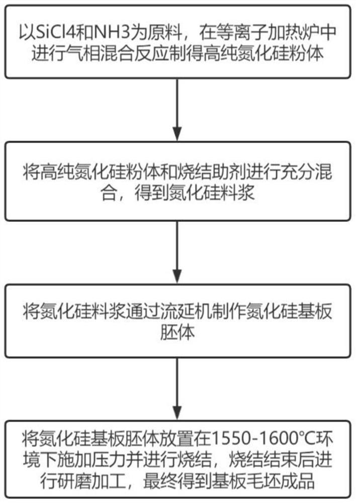
[0026] refer to figure 1 As shown, an embodiment of the method for preparing a high thermal conductivity silicon nitride ceramic substrate for a high power integrated circuit of the present invention includes the following steps:

[0027] First, prepare high-purity silicon nitride powder with SiCl 4 and NH 3 As raw material, the gas phase mixing reaction is carried out in a plasma heating furnace to obtain high-purity silicon nitride powder, SiCl 4 and NH 3 The purity is above 99.99%; the chemical reaction formula is 3SiCl 4 +4NH 3 →Si 3 N 4 +12HCl; By abandoning the traditional silicon nitride powder synthesis process, using plasma chemical vapor deposition method, using SiCl ...


PUM

PropertyMeasurementUnit
thicknessaaaaaaaaaa
strengthaaaaaaaaaa
strengthaaaaaaaaaa

Abstract

The invention discloses a preparation method of a high-thermal-conductivity silicon nitride ceramic substrate for a high-power integrated circuit, which comprises the following steps: preparing high-purity silicon nitride powder, taking S C < 14 > and NH3 as raw materials, and carrying out gas-phase mixing reaction in a plasma heating furnace to prepare the high-purity silicon nitride powder with the purity of S C < 14 > and NH3 being 99.99% or above; the chemical reaction formula is 3S C < 14 > + 4NH3-> S N < 4 > + 12HC < 1 >; then preparing silicon nitride slurry, fully mixing the high-purity silicon nitride powder and a sintering aid to obtain a mixed material, and mixing the mixed material with the carrier solution to obtain the silicon nitride slurry; carrying out substrate forming, and manufacturing the silicon nitride slurry through a casting machine to obtain a silicon nitride substrate blank; and finally, carrying out low-temperature pressure sintering, namely sintering the silicon nitride substrate blank subjected to tape casting in an environment of 1550-1600 DEG C, applying a mechanical pressure of 20-30 MPa to the silicon nitride substrate blank while sintering, and carrying out grinding processing after the sintering is finished, so as to finally obtain a finished product of the substrate blank. The thermal conductivity is high, the strength is good, the cost is effectively controlled, and industrial popularization can be carried out.

Description

technical field [0001] The invention relates to the technical field of preparation of silicon nitride ceramic substrates, in particular to a preparation method of a high thermal conductivity silicon nitride ceramic substrate for high-power integrated circuits. Background technique [0002] With the increasing integration of semiconductor devices, the generation of a large amount of heat is a key factor that causes the failure of the semiconductor device. The thermal conductivity of the circuit substrate used in the semiconductor device is the key to affecting the heat dissipation of the overall semiconductor device. Therefore, it is required that the circuit must have the following characteristics: high strength, high hardness, high resistivity, good thermal shock resistance, low dielectric loss and low expansion coefficient, and it must also meet the bumps in high-speed rail, electric vehicles and other fields. Vibration and other complex mechanical environment requirements...

Claims


Application Information

Patent Timeline
Patent Type & Authority Applications(China)
IPC IPC(8): C04B35/596C04B35/622C04B35/626C04B35/64
CPCC04B35/587C04B35/622C04B35/626C04B35/64C04B2235/3225C04B2235/3227C04B2235/3229C04B2235/3217C04B2235/656C04B2235/6567C04B2235/96C04B2235/9607
Inventor 杨双收鲁盛会刘得顺滕红卫王斌熊加丽杨梦格刘雁飞王财玲刘璐
Owner 秦皇岛光岩科技有限公司
Learn More