Phototransistor preparation method based on femtosecond laser and transistor array

A technology of phototransistors and femtosecond lasers, applied in circuits, electrical components, semiconductor devices, etc., can solve problems such as the inability to guarantee the stability of transistor devices, reduce uncertain factors, improve uniformity and stability, and reduce preparation processes cost effect

Pending Publication Date: 2022-08-05
CENT SOUTH UNIV
View PDF0 Cites 0 Cited by
  • Summary
  • Abstract
  • Description
  • Claims
  • Application Information

AI Technical Summary

Problems solved by technology

[0004] The preparation method of phototransistor based on femtosecond laser provided by the present invention solves the technical problem that the stability of the transistor device cannot be guaranteed in the existing transistor device manufactured by photolithography technology using a physical mask

Method used


Image

  • Phototransistor preparation method based on femtosecond laser and transistor array
  • Phototransistor preparation method based on femtosecond laser and transistor array
  • Phototransistor preparation method based on femtosecond laser and transistor array

Examples


preparation example Construction

[0029] Please refer to figure 1 , image 3 , Figure 4 and Figure 5 , a method for preparing a phototransistor based on a femtosecond laser in a preferred embodiment provided by the present invention includes the steps:

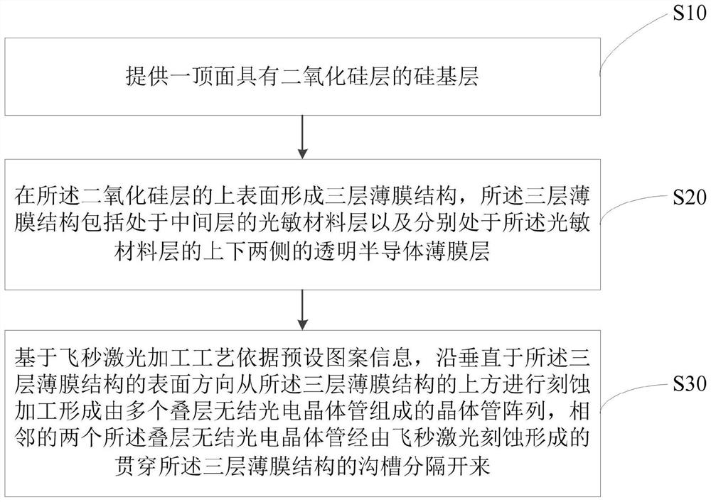
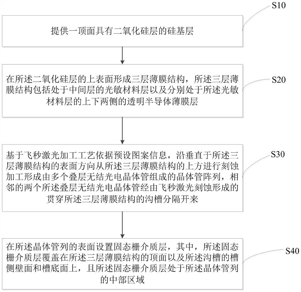
[0030] S10, providing a silicon base layer with a silicon dioxide layer on the top surface;

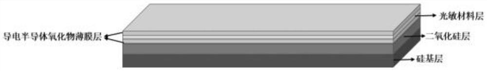
[0031] S20, a three-layer thin film structure is formed on the upper surface of the silicon dioxide layer, and the three-layer thin film structure includes a photosensitive material layer in the middle layer and a transparent semiconductor thin film layer (transparent conductive semiconductor oxide thin film on the upper and lower sides of the photosensitive material layer, respectively). Floor);

[0032] S30, based on a femtosecond laser processing process and according to preset pattern information, etching is performed from above the three-layer thin-film structure along a surface direction perpendicular to the three-layer thin-film structure to form a transi...

Embodiment approach

[0058] The present invention provides a specific embodiment as follows:

[0059] Select heavily doped P-type silicon with 300nm thermally grown silicon dioxide (gate dielectric) on it as the substrate, select indium tin oxide (ITO) thin film layer for the transparent semiconductor film (heavy doped semiconductor layer) layer, and select photosensitive material for the photosensitive material. Quantum dots, solid-state ionic electrolytes and selective ionic liquids.

[0060] The fabrication method of phototransistor based on femtosecond laser includes the following steps:

[0061] Step 1: successively use acetone, alcohol and deionized water to ultrasonically clean the heavily doped silicon wafer substrate with 300nm thermally grown silicon dioxide and perform drying treatment;

[0062] Step 2: put the silicon wafer substrate (silicon base layer) into the vacuum chamber of radio frequency magnetron sputtering, and deposit a layer of transparent ITO thin film as a heavily doped s...


PUM

PropertyMeasurementUnit
Thicknessaaaaaaaaaa
Thicknessaaaaaaaaaa

Abstract

The invention discloses a femtosecond laser-based phototransistor preparation method and a transistor array. Comprising the following steps: S10, providing a silicon-based layer with a silicon dioxide layer on the top surface; s20, forming a three-layer film structure on the upper surface of the silicon dioxide layer; and S30, on the basis of a femtosecond laser processing technology and according to preset pattern information, etching processing is carried out from the upper portion of the three-layer thin film structure in the direction perpendicular to the surface of the three-layer thin film structure to form a transistor array composed of a plurality of laminated junctionless phototransistors, and the adjacent laminated junctionless phototransistors are separated through grooves. According to the femtosecond laser-based phototransistor preparation method, a femtosecond laser micro-nano processing technology is used, and a photoetching step in a traditional patterning process is omitted, so that the preparation process cost of a transistor device is reduced, and a photosensitive material and a semiconductor material are compounded; photo-generated carriers are injected into a semiconductor to improve the mobility of device electrons and holes, and higher photocurrent response is obtained.

Description

1Technical field [0001] The present invention relates to the technical field of semiconductors, and in particular, to a preparation method and an array of a phototransistor based on a femtosecond laser. 2 Background technology [0002] The pattern transfer process of the traditional micromachining process requires the use of photolithography technology, which usually requires the use of a physical mask, and the pattern on the mask is copied to the substrate by ultraviolet light, and then developed to form the required pattern. The traditional micromachining process steps are cumbersome, and various defects are easily introduced during the process due to unstable process equipment or factors such as sanitation and incomplete cleaning steps, and the stability and low cost of transistor devices cannot be guaranteed. [0003] In order to improve the problems of transistor fabrication process and device performance, it is necessary to propose a femtosecond laser-based phototransi...

Claims


Application Information

Patent Timeline
IPC IPC(8): H01L31/112H01L31/18
CPCH01L31/112H01L31/1804Y02P70/50
Inventor 蒋杰张艺黄卓慧银恺
Owner CENT SOUTH UNIV
Why Eureka
Try Eureka