HEMT epitaxial structure with low buffer layer leakage current and HEMT device

A technology of epitaxial structure and leakage current, which is applied in the direction of electrical components, semiconductor devices, circuits, etc., can solve the problems of increasing the leakage current of the buffer layer, high leakage current of the buffer layer, and easy breakdown, so as to reduce leakage and improve breakdown Voltage, crack prevention effect

Pending Publication Date: 2022-08-09
XIDIAN UNIV
View PDF0 Cites 0 Cited by
  • Summary
  • Abstract
  • Description
  • Claims
  • Application Information

AI Technical Summary

Problems solved by technology

The current method to improve the performance of silicon-based HEMT devices is to increase the thickness of the GaN buffer layer on the substrate, but this method is difficult to control, with low yield and high cost
Moreover, the silicon substrate that is not completely insulated will provide electrons to the buffer layer, and the substrate electrons entering the buffer layer will increase the leakage current of the buffer layer, resulting in a high leakage current in the buffer layer of silicon-based HEMT devices, which is prone to breakdown, resulting in device damage

Method used


Image

  • HEMT epitaxial structure with low buffer layer leakage current and HEMT device
  • HEMT epitaxial structure with low buffer layer leakage current and HEMT device
  • HEMT epitaxial structure with low buffer layer leakage current and HEMT device

Examples


Embodiment 1

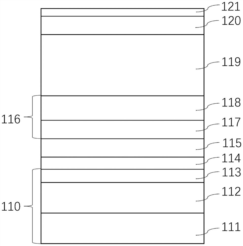
[0028] See figure 1 In the first aspect of the embodiment of the present invention, a HEMT epitaxial structure with low buffer layer leakage current is provided, including: a silicon substrate 110, an AlN nucleation layer 114, a back barrier electron blocking layer 115, a stress regulation and control layer arranged in order from bottom to top layer 116 , GaN high resistance layer 119 , GaN channel layer 120 and barrier layer 121 . The epitaxial structure can be grown by epitaxial growth techniques such as metal organic chemical vapor deposition (MOCVD) and molecular beam epitaxy (MBE).

[0029] The silicon substrate 110 includes: a first sub-substrate 111 , a second sub-substrate 112 and a third sub-substrate 113 arranged in sequence from bottom to top. Specifically, the AlN nucleation layer 114 is located on the third sub-substrate 113 .

[0030] The type of carriers (majority carriers) of the first sub-substrate 111 is opposite to the type of carriers (majority carriers) ...

Embodiment 2

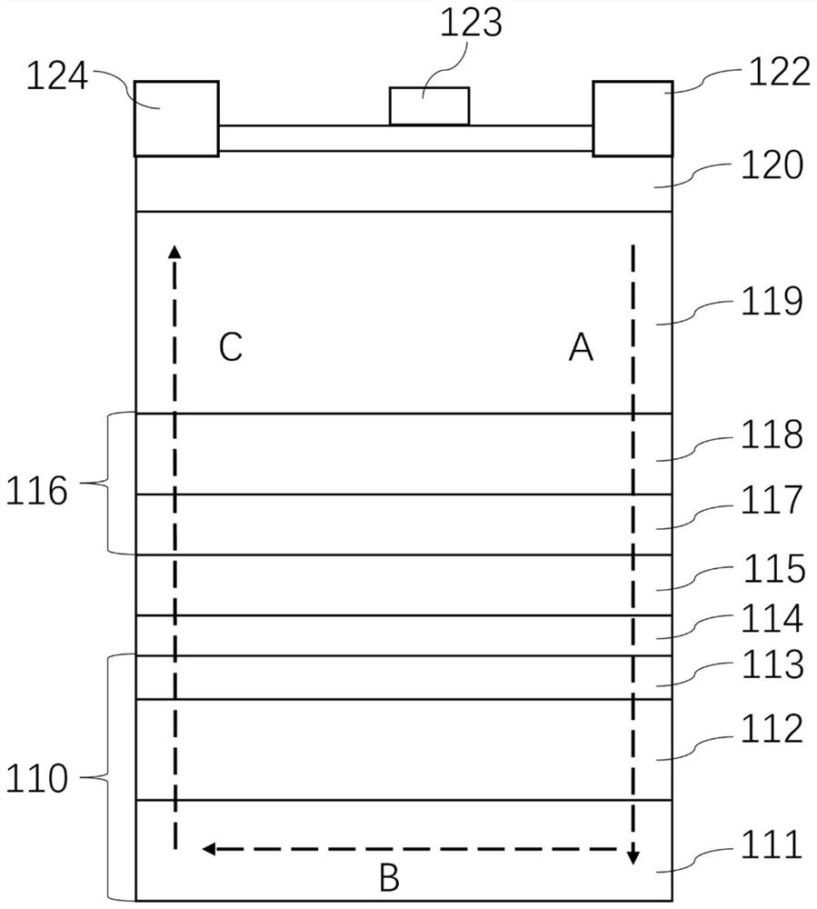
[0043] like figure 2 As shown, the second aspect of the embodiment of the present invention further provides a HEMT device with low buffer layer leakage current, including the source electrode 124 , the drain electrode 122 , the gate electrode 123 and the epitaxial structure in the first embodiment.

[0044] The source electrode 124 and the drain electrode 122 are located on the GaN channel layer 120 of the epitaxial structure and on both sides of the barrier layer 121 of the epitaxial structure, and the gate electrode 123 is located on the barrier layer 121 and between the source electrode 124 and the drain electrode 122 . Specifically, the drain electrode 122 and the source electrode 124 are deposited by electron beam evaporation process to form ohmic contact with two-dimensional electron gas of the channel layer, and the gate electrode 123 is deposited by electron beam evaporation process to form Schottky contact, and finally the HEMT device is prepared.

[0045] like f...

Embodiment 3

[0047] In one embodiment of the present invention, a HEMT epitaxial structure with low buffer layer leakage current includes: a silicon substrate 110 , an AlN nucleation layer 114 , a back barrier electron blocking layer 115 , and a stress control layer arranged in order from bottom to top layer 116 , GaN high resistance layer 119 , GaN channel layer 120 and barrier layer 121 . Among them, the epitaxial structure can complete the growth of each layer by metal organic chemical vapor deposition (MOCVD).

[0048] The silicon substrate 110 includes: a first sub-substrate 111 , a second sub-substrate 112 and a third sub-substrate 113 arranged in sequence from bottom to top. Specifically, the AlN nucleation layer 114 is located on the third sub-substrate 113 . P-type Si is selected as the first sub-substrate 111, and the first majority carrier concentration is 2.0×10 15 cm -3 , the part above the upper surface of the first sub-substrate 111 is doped with n-type by means of ion im...


PUM

PropertyMeasurementUnit
thicknessaaaaaaaaaa
thicknessaaaaaaaaaa
thicknessaaaaaaaaaa

Abstract

The invention discloses an HEMT epitaxial structure with low buffer layer leakage current. The HEMT epitaxial structure comprises a silicon substrate, an AlN nucleating layer, a back barrier electron barrier layer, a stress regulation and control layer, a GaN high-resistance layer, a GaN channel layer and a barrier layer which are sequentially arranged from bottom to top, the silicon substrate comprises a first sub-substrate, a second sub-substrate and a third sub-substrate which are sequentially arranged from bottom to top; and the back barrier electron barrier layer is of a periodically epitaxial Al < x > Ga < 1-x > N/Al < y > Ga < 1-y > N superlattice structure. The invention also provides an HEMT device with low buffer layer leakage current. According to the invention, the first sub-substrate and the second sub-substrate are contacted to form a PN junction, and an inversion electron layer is prevented from being formed on the interface of the silicon substrate and the AlN nucleating layer, so that electrons of the silicon substrate are prevented from entering the stress regulation and control layer, and the electric leakage of the buffer layer is reduced. Meanwhile, the back barrier electron barrier layer with the superlattice structure can effectively improve the barrier between the interface of the AlN/Si substrate and the stress regulation and control layer, prevents substrate electrons from being injected into the stress regulation and control layer, and reduces the electric leakage of the stress regulation and control layer.

Description

technical field [0001] The invention belongs to the technical field of nitride electronic devices, in particular to a HEMT epitaxial structure with low buffer layer leakage current and a HEMT device. Background technique [0002] In recent years, the electronic transformation of almost the whole industry has greatly increased the social demand for electronic power devices. Since the invention of the first GaN-based electronic device, the high electron mobility transistor (HEMT) with AlGaN / GaN heterojunction as the core has developed rapidly in the past two decades. However, the current GaN-based electronic device is expensive and the market space Small, large-size silicon substrate can greatly reduce the cost, but the huge lattice mismatch and thermal expansion coefficient difference between Si and GaN will cause the subsequent epitaxial layer to bear huge tensile stress, which will cause high-density dislocations. Some dislocations even run through the entire epitaxial lay...

Claims


Application Information

Patent Timeline
Patent Type & Authority Applications(China)
IPC IPC(8): H01L29/06H01L29/20H01L29/778
CPCH01L29/0615H01L29/0684H01L29/2003H01L29/778
Inventor 李培咸刘瑞宇周小伟黄晨曦
Owner XIDIAN UNIV
Why Eureka
Try Eureka