LED chip and preparation method thereof

A LED chip and graphic technology, applied in semiconductor devices, electrical components, circuits, etc., can solve the problems of low light extraction efficiency, achieve the effects of improving safety performance, increasing reflectivity, and slowing down overheating

Pending Publication Date: 2022-08-09
JIANGXI ZHAO CHI SEMICON CO LTD
View PDF0 Cites 0 Cited by
  • Summary
  • Abstract
  • Description
  • Claims
  • Application Information

AI Technical Summary

Problems solved by technology

[0004] Based on this, the purpose of the present invention is to propose an LED chip and its preparation method to solve the problem of low light extraction efficiency of traditional LED chips due to the serious light absorption phenomenon, which is conducive to improving the luminous brightness of large-angle chips

Method used


Image

  • LED chip and preparation method thereof
  • LED chip and preparation method thereof

Examples


Embodiment 1

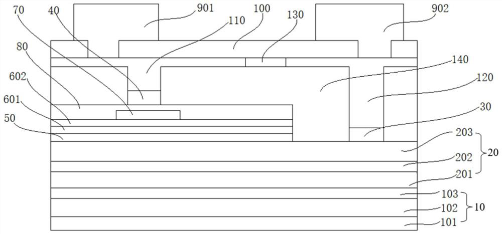
[0034] see figure 1 , which is a schematic structural diagram of the LED chip provided by the first embodiment of the present invention, the LED chip includes a composite substrate substrate 10, an epitaxial layer group and a contact layer group stacked in sequence, wherein:

[0035] The epitaxial layer set includes a first semiconductor layer 20 , a light-emitting layer 50 and a second semiconductor layer sequentially stacked on the composite substrate 10 . the conductive groove of the second semiconductor layer;

[0036]The contact layer set includes a current blocking layer 70 disposed on the second semiconductor layer, a current guiding layer 80 completely covering the current blocking layer 70, and a first patterned reflective layer 140 disposed in the conductive groove , and the first patterned reflective layer 140 is disposed on the first semiconductor layer 20 and the current guide layer 80. The purpose of setting the first patterned reflective layer 140 is to prevent...

Embodiment 2

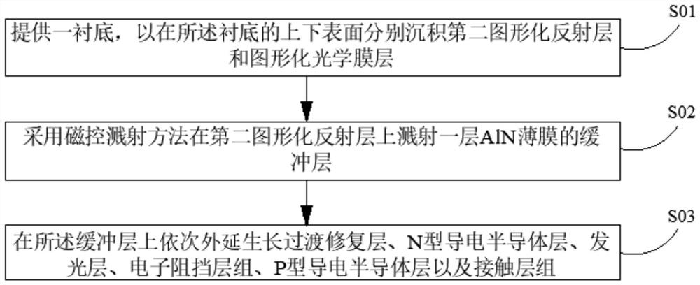
[0049] see figure 2 , which is a flow chart of a method for preparing an LED chip in the second embodiment of the present invention. The method is used to prepare the LED chip in the above-mentioned embodiment, and the method includes steps S01 to S03, wherein:

[0050] Step S01: providing a substrate for depositing a second patterned reflective layer and a patterned optical film layer on the upper and lower surfaces of the substrate respectively;

[0051] Specifically, a second patterned reflective layer is deposited on the upper surface of the substrate by means of PECVD (Plasma Enhanced Chemical Vapor Deposition). A plurality of grooves with a depth less than half of the thickness of the second patterned reflective layer are etched on the side of the second patterned reflective layer away from the substrate, and then PECVD (plasma enhanced chemical vapor deposition) method is used again on the substrate. Silicon dioxide layers and titanium pentoxide layers are alternately...


PUM

PropertyMeasurementUnit
thicknessaaaaaaaaaa
thicknessaaaaaaaaaa
thicknessaaaaaaaaaa

Abstract

The LED chip comprises a substrate, a heat conduction substrate, an epitaxial layer and an electrode contact layer, a second current guiding layer is arranged on the surface of a second type semiconductor layer, a first groove penetrating through the second current guiding layer is formed in the second current guiding layer, and a second current guiding layer is arranged in the first groove. The current blocking layer is arranged in the first groove and makes contact with the surface of the second type semiconductor layer, the third current guiding layer is arranged on the current blocking layer, the current blocking layer and the third current guiding layer are provided with a plurality of second grooves penetrating through the current blocking layer and the third current guiding layer, the fourth current guiding layer is arranged on the side wall of the second groove, and the fourth current guiding layer is arranged on the side wall of the second groove. The second conductive electrode is arranged on the second current guiding layer, the third current guiding layer and the fourth current guiding layer and extends downwards to the second groove. According to the LED chip provided by the invention, the luminous efficiency and the luminous efficiency of a product can be greatly improved.

Description

technical field [0001] The invention relates to the technical field of semiconductor manufacturing, in particular to an LED chip and a preparation method thereof. Background technique [0002] In recent years, light-emitting diodes have shown great advantages in white light lighting, display screens, ultraviolet disinfection and other industries due to their advantages of energy saving, environmental protection, long life and fast response. With the advent of the global energy crisis, the concept of energy saving and environmental protection is deeply rooted in the hearts of the people. [0003] In the prior art, large-angle light-emitting diodes are widely favored by the market because of their better uniformity of light output. emitting light, which further aggravates the phenomenon of absorbing light, which in turn leads to low light emitting efficiency of the large-angle light emitting diode, thereby affecting the luminous brightness. SUMMARY OF THE INVENTION [0004...

Claims


Application Information

Patent Timeline
Patent Type & Authority Applications(China)
IPC IPC(8): H01L33/06H01L33/14H01L33/38H01L33/46H01L33/62
CPCH01L33/06H01L33/145H01L33/46H01L33/387H01L33/62H01L2933/0066
Inventor 曹斌斌胡加辉金从龙
Owner JIANGXI ZHAO CHI SEMICON CO LTD
Why Eureka
Try Eureka