Method for thinning scribing of sapphire group nitride chip

A nitride, sapphire technology, applied in semiconductor lasers, lasers, semiconductor devices, etc., can solve the problems of small laser absorption, unfavorable laser scribing efficiency, damage to the optoelectronic properties of GaN/sapphire LED chips, etc., to overcome high hardness, improve thinning effect

Inactive Publication Date: 2006-12-27
SHANGHAI INST OF OPTICS & FINE MECHANICS CHINESE ACAD OF SCI
View PDF1 Cites 0 Cited by
  • Summary
  • Abstract
  • Description
  • Claims
  • Application Information

AI Technical Summary

Problems solved by technology

However, there are also problems with laser scribing: (1) Since sapphire is a transparent medium, its absorption of laser light is very small, which is not conducive to improving the efficiency of laser scribing; (2) The thermal effect generated by laser cutting may damage GaN / sapphire Photoelectric properties of LED chips

Method used


Image

  • Method for thinning scribing of sapphire group nitride chip

Examples


Embodiment Construction

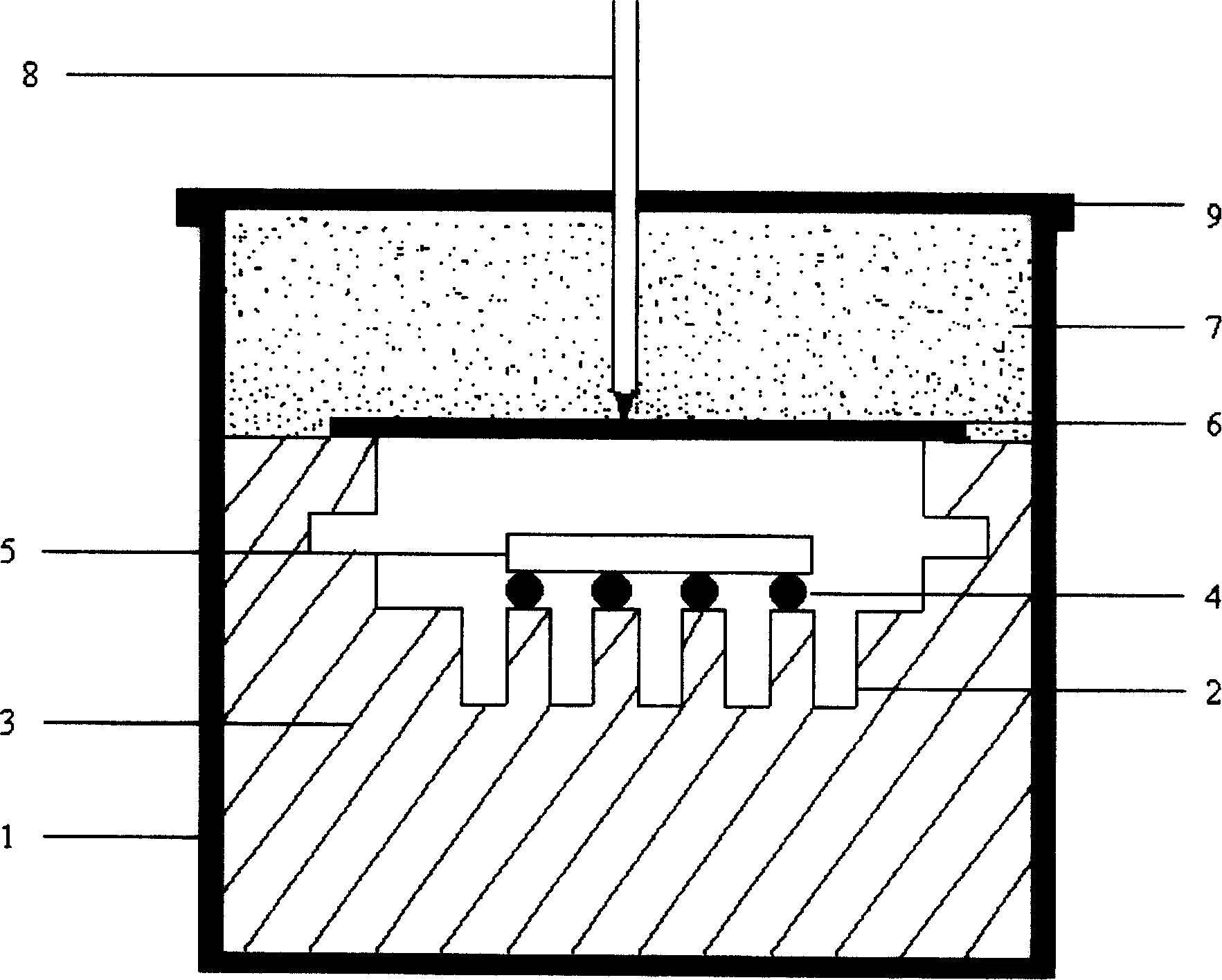
[0024] The schematic diagram of crucible structure of gas phase transport equilibrium (VTE) technology used in the present invention is as figure 1 As shown, in the platinum crucible 1, a certain ratio of γ-LiAlO with pores 2 is placed 2 and Li 2 O mixed material block 3, the upper part of the material block 3 is platinum wire 4, the nitride chip sandwich cake 5 is placed on the platinum wire 4, and the upper part of the material block 3 has platinum sheet 6 and γ-LiAlO 2 and Li 2 O The mixed powder 7 is covered, the thermocouple 8 is inserted into the mixed powder 7, and the top of the crucible 1 is sealed with a platinum cover 9.

[0025] Vapor transport equilibrium (VTE) is a mass transport process, so there should be enough Li in the crucible 2 O supply; secondly, the balance of the gas phase is dependent on Li 2 A steady stream of O from γ-LiAlO 2 and Li 2 O is maintained by volatilization in the mixture block, in order to prevent Li on the surface of the mixture bl...


PUM


Abstract

The invention is a method of thinning and scribing a sapphire-based nitride chip, including the following steps: in pairs pasting the chip into a cake with filling; sending the cake into a platinum crucible and placing or hanging the crucible on a platinum wire, placing holed gama-LiAiO2 and Li2O mixed block in the crucible, where there is platinum piece on the top of the block and the platinum piece is covered with gama-LiAiO2 and Li2O mixed powder and the crucible is set with a cover with a thermal couple, the top of the crucible is closed by a platinum cover, and place the crucible in a resistance furnace: the resistance furnace is heated to 750-900 deg.C and keep the temperature 80-200 hours, Li2O diffuses into the sapphire wafer to make solid-phase reaction to generate lithium aluminate (gama-LiAlO2); by mechanical or chemical method, thin the nitride chip, split the cake with filling in the middle; scribe; crack; test, classify and package the chip. It enhances thinning and scribing efficiency and yield.

Description

technical field [0001] The invention relates to a method for thinning and dicing a sapphire-based nitride chip. Thinning dicing is an important step in cutting GaN / sapphire LED chips. Background technique [0002] Wide bandgap III-V compound semiconductor materials represented by GaN are receiving more and more attention, and they will be used in blue and green light-emitting diodes (LEDs) and laser diodes (LDs), high-density information reading and writing, underwater It has broad application prospects in communication, deep water exploration, laser printing, biological and medical engineering, ultra-high-speed microelectronic devices and ultra-high-frequency microwave devices. [0003] At present, ultra-high brightness GaN / sapphire LEDs are more and more widely used in indoor and outdoor color display, traffic signal indication, LED background light source and white lighting source, and its production scale is rapidly expanding. In the production process, the GaN / sapphir...

Claims


Application Information

Patent Timeline
Patent Type & Authority Patents(China)
IPC IPC(8): H01L33/00H01S5/00H01L21/302
Inventor 徐军彭观良周圣明周国清蒋成勇王海丽李抒智赵广军张俊计刘军芳邹军王银珍吴锋庄漪
Owner SHANGHAI INST OF OPTICS & FINE MECHANICS CHINESE ACAD OF SCI
Why Eureka
Try Eureka