Ferroelectric FET and its preparing process

An electric field effect and transistor technology, which is applied in the field of microelectronic devices, can solve problems such as fatigue and poor interface characteristics, and achieve the effects of simplifying the process, improving the yield, and realizing non-volatile storage

Inactive Publication Date: 2002-07-03
HUAZHONG UNIV OF SCI & TECH
View PDF0 Cites 14 Cited by
  • Summary
  • Abstract
  • Description
  • Claims
  • Application Information

AI Technical Summary

Problems solved by technology

[0007] The purpose of the present invention is to provide a novel ferroelectric field effect transistor, which can overcome the shortcomings of poor interface characteristics and fatigue of general ferroelectric memory effect devices, and has good storage performanc

Method used


Image

  • Ferroelectric FET and its preparing process
  • Ferroelectric FET and its preparing process
  • Ferroelectric FET and its preparing process

Examples


Embodiment Construction

[0019]The present invention will be described in further detail below in conjunction with the accompanying drawings.

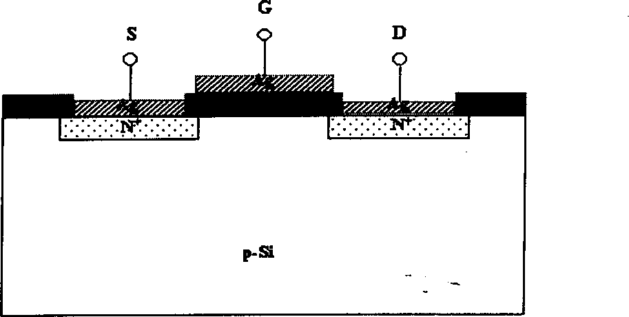
[0020] Such as figure 1 As shown, the ferroelectric field effect transistor can be divided into several identical unit segments, and the unit segment is composed of a substrate 1, a source region 2, a drain region 4, and a gate region 3 between the source region 2 and the drain region 4, The substrate 1 is a P-type single crystal silicon wafer with a (100) crystal orientation, and the source region 2 and the drain region 4 are N + The ion implantation area is embedded in the surface of the substrate 1, and the gate area 3 is bismuth titanate Bi 4 Ti 3 o 12 The thin film is located on the upper surface of the substrate 1, and there is a layer of Ag electrodes on the surfaces of the source region 2, the gate region 3 and the drain region 4, which form the source electrode 5, the gate electrode 6 and the drain electrode 7 respectively.

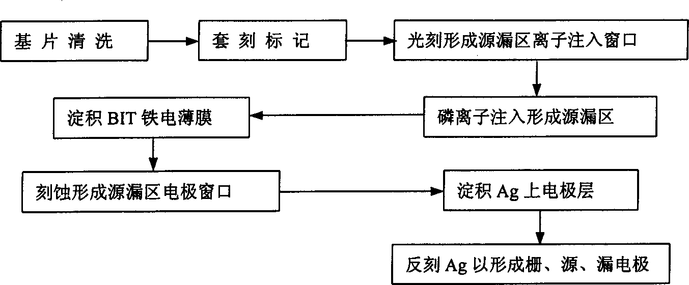
[0021] The preparatio...


PUM


Abstract

A ferroelectric FET with bismuth titanate (BIT) film as storage medium layer is prepared through washing Si substrate, coating photoresist, exposing, developing to obtain pattern, etching to form recess, coating photoresist, phootoetching to form injection windows of source and drain areas, ion implantation to form source and drain areas, depositing ferroelectric BIP film, etching off the film over source and drain areas to obtain the windows of source and drain, plating AG layer, and reverse etching to obtain source, drain and grid. Its advantages include good interface performance, long information storage time and high rate of finished products.

Description

technical field [0001] The invention belongs to the field of microelectronic devices, and specifically relates to a ferroelectric field effect transistor, in particular to a nonvolatile, Ag / BIT gate ferroelectric field effect transistor; the invention also relates to a preparation method of the ferroelectric field effect transistor. Background technique [0002] The ferroelectric field effect transistor (hereinafter referred to as "FFET") uses the MFIS (Metal / Ferroelectric / Insulator / Semiconductor) structure as the basic storage unit, which replaces the gate dielectric layer in the semiconductor field effect transistor with a ferroelectric film, and passes the gate polarization (±P r ) realizes the modulation of the source-drain current, making it significantly increase or decrease. When a write pulse is applied to the gate, the ferroelectric film is permanently polarized, and the source and drain are turned on to a "1" state. If a reverse pulse is applied, the channel is tu...

Claims


Application Information

Patent Timeline
IPC IPC(8): H01L21/335H01L29/772
Inventor 于军王华王耘波周文利周东祥刘刚谢基凡高俊雄
Owner HUAZHONG UNIV OF SCI & TECH
Why Eureka
Try Eureka