Method for producing semi-conductor device

A semiconductor and device technology, applied in the field of semiconductor device manufacturing, can solve problems such as poor consistency and unsuitable glass substrates, and achieve the effect of controlling and reducing concentration

Inactive Publication Date: 2002-07-31
SEMICON ENERGY LAB CO LTD
View PDF1 Cites 5 Cited by
  • Summary
  • Abstract
  • Description
  • Claims
  • Application Information

AI Technical Summary

Problems solved by technology

Therefore, crystallization by heat treatment at the above-mentioned high temperature is not suitable for glass substrates.
On the other hand, although short-pulse lasers such as excimer lasers have the advantage of not deforming the glass substrate, the uniformity of device characteristics is not so good when using lasers

Method used


Image

  • Method for producing semi-conductor device
  • Method for producing semi-conductor device
  • Method for producing semi-conductor device

Examples


Embodiment 1

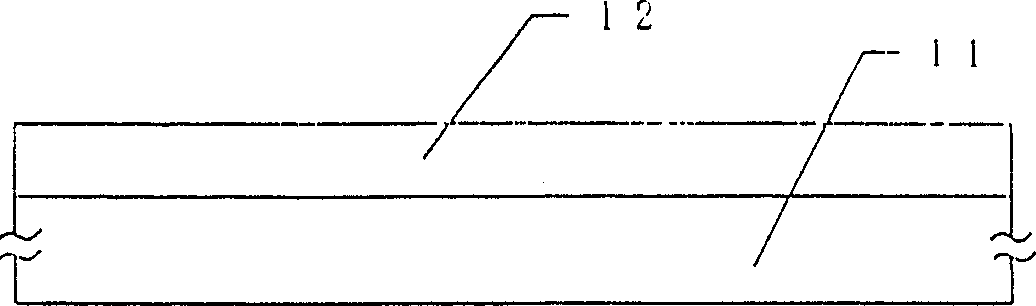
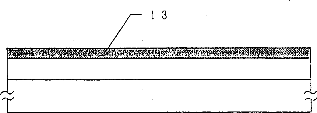
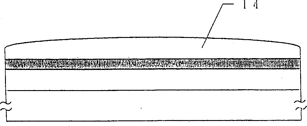
[0060] In this example, reference will be made to Figure 1A -1D discusses the process of heating and crystallizing a semiconductor film formed from an aqueous solution containing a catalyst, followed by crystallization by laser irradiation.

[0061] Prior to laser crystallization, the concentration of hydrogen contained in the amorphous silicon film should be as small as possible, for example, from 0.01 to 10 percent atmospheric pressure. Therefore, in order to release hydrogen from the silicon film, it is preferable to heat the amorphous silicon film at a temperature lower than the crystallization temperature. In an alternative, use 100-500 sccm of Si 2 h 6 Silane and 500 sccm of helium are used to form an amorphous silicon film by low pressure chemical vapor deposition at a relatively high temperature, for example, 430-500° C., wherein the concentration of hydrogen is within the above-mentioned range.

[0062] exist Figure 1A , reference numeral 11 denotes a Corning 7059...

Embodiment 2

[0072] This embodiment is exactly the same as the previous embodiment except that the concentration of nickel in the solution is changed to 1 ppm.

[0073] The silicon film in this example was observed with a microscope after the heat treatment, and as a result, it was found that the portion of the amorphous silicon film was larger than that of the above example, and the crystal nuclei were reduced.

[0074] Further, after laser crystallization, the sample was subjected to Secco-etched and observed with a scanning electron microscope. As a result, it was found that the size of each crystal was larger than that obtained in the previous example.

Embodiment 3

[0076] The present embodiment relates to a process for producing a TFT for a plurality of pixels of an active matrix liquid crystal display device or for a driving circuit using a crystalline silicon film produced by the process of the present invention. TFTs can be used not only in liquid crystal display devices but also in a wide range of fields generally called thin film integrated circuits (ICs).

[0077] see Figures 3A-3E , the process of manufacturing a TFT according to this embodiment will be described below. A silicon oxide film (not shown in the figure) was deposited to a thickness of 2000 Å as a base layer on the glass substrate. This silicon oxide layer is used to prevent impurities from penetrating the device from the glass substrate.

[0078] Then, in the same manner as in Example 1, an amorphous silicon film was deposited to a thickness of 500 Å. After removing the natural oxide film by treatment with hydrofluoric acid, an oxide film was formed to a thickness...


PUM

PropertyMeasurementUnit
thicknessaaaaaaaaaa
strengthaaaaaaaaaa

Abstract

A method of manufacturing a semiconductor device which has a crystalline silicon film comprises the steps of forming crystal nuclei in a surface region of an amorphous silicon film and then growing the crystals from the nuclei by a laser light. Typically the crystal nuclei are silicon crystals or metal suicides having an equivalent structure as silicon crystal.

Description

[0001] This application is a divisional application of a patent application with an application date of February 3, 1995 and an application number of 95102929.0. technical field [0002] The present invention relates to a semiconductor device having a crystalline semiconductor material and a method of manufacturing the same. Background technique [0003] Thin film transistors fabricated using thin film semiconductors formed on a substrate are known. Such thin-film transistors (TFTs) are used in integrated circuits, especially in electro-optic devices such as active matrix liquid crystal devices, as switching elements for each pixel or as drivers in peripheral circuits that drive active matrix elements. element. [0004] Amorphous silicon films for TFTs are readily available. However, the electrical properties of amorphous silicon films are poor. Therefore, it is desirable to use a semiconductor film having crystallinity, that ...

Claims


Application Information

Patent Timeline
Patent Type & Authority Applications(China)
IPC IPC(8): C30B29/06C30B1/00C30B30/00H01L21/02H01L21/20H01L21/268H01L21/336H01L27/00H01L27/01H01L27/12H01L29/78H01L29/786
CPCH01L29/66757H01L21/2026H01L21/0262H01L21/02592H01L21/02686H01L21/02488H01L21/02422H01L21/02532H01L21/0242H01L21/02672H01L21/20H01L21/02675H01L21/02667
Inventor 大谷久宫永昭治竹山顺一
Owner SEMICON ENERGY LAB CO LTD
Why Eureka
Try Eureka