2D photon Si-base crystal waveguide don insulator with dual insulating burried layers and its preparing process

A two-dimensional photonic crystal and photonic crystal waveguide technology, applied in the field of optoelectronics, can solve the problems of narrow photonic band gap, small dielectric constant, poor repeatability, etc., and achieve the effect of good single crystal quality, low energy loss and good quality

Inactive Publication Date: 2002-12-04
SHANGHAI SIMGUI TECH
View PDF0 Cites 16 Cited by
  • Summary
  • Abstract
  • Description
  • Claims
  • Application Information

AI Technical Summary

Problems solved by technology

H.Miguez et al prepared photonic crystals by uniformly mixing medium particles into a special solution to self-organize. The disadvantages are that the dielectric constant is relatively small and the photonic band gap is narrow (H.Miguez et al.Appl.Phys.Lett.1997, 71:1148 -1150)
Another disadvantage of the self-organized growth method is poor reproducibility
[0006] In addition, there are also photonic crystal waveguides based on air bridge structures. Although this waveguide can increase the filling ratio of air, it is difficult to realize large-scale devices or integrate with other functional components.

Method used


Image

  • 2D photon Si-base crystal waveguide don insulator with dual insulating burried layers and its preparing process
  • 2D photon Si-base crystal waveguide don insulator with dual insulating burried layers and its preparing process
  • 2D photon Si-base crystal waveguide don insulator with dual insulating burried layers and its preparing process

Examples


Embodiment 1

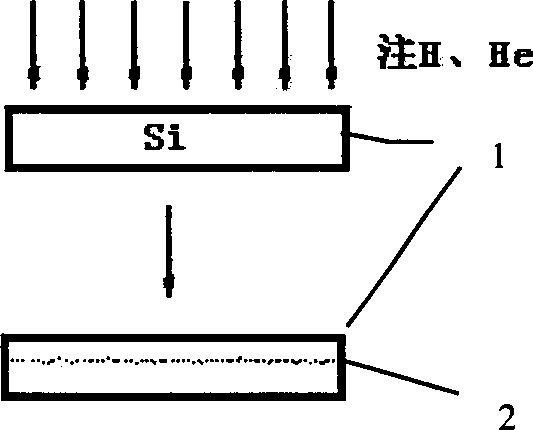
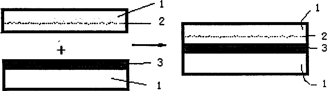
[0036] The high-quality SOI prepared by the improved Smart-Cut method is used as the substrate of the two-dimensional photonic crystal. First implant the energy of 30KeV into the single crystal silicon wafer 1, and the dose is 1×10 16 / cm 2 H + , the re-implantation energy is 33KeV, and the dose is 1×10 16 / cm 2 He + ; During implantation, the ion beam deviates from the normal line of the sample by 7°, while keeping the temperature of the target below 200°C during the implantation process; the support sheet adopts a double buried layer (SiO 2 / Si 3 N 4 ), SiO 2 Prepared by ultra-high vacuum electron beam evaporation (UHV-EBE), the substrate temperature is 200 ° C, Si 3 N 4 Low-pressure chemical vapor deposition (LPCVD) is used, and the substrate temperature is 1000°C. Then bond, and then heat-treat the bonded sheet at 520°C, the sheet is cracked from the bubble layer 2 and facet formed by H and He injection: annealing at 1100°C strengthens the bond and forms a high-q...

Embodiment 2

[0039] In order to obtain two-dimensional photonic crystal waveguides with different photonic band gaps, in the air holes of the two-dimensional photonic crystal waveguides formed in method 1, deposit other dielectric materials (SiO 2 ,TiO 2 , Ta 2 o 5 etc.), such as using UHV-EBE method to grow 1μm thick TiO 2 ( Figure 10 )5, the background vacuum of the target chamber reaches 10 -8 ~10 -9 Torr, the substrate temperature is 200°C, and the growth rate is 1 Å / s; the surface is then CMPed to form a two-dimensional photonic crystal waveguide ( Figure 11 ).

Embodiment 3

[0041] The double buried layer used in the support sheet is SiO 2 / AlN, SiO 2 Formation of 0.8μm SiO by thermal oxidation 2 layer, AlN is deposited by low-pressure chemical vapor deposition (LPCVD), the substrate temperature is 900°C, the thickness is 1.2 μm, and the total thickness of the double insulating buried layer is 2 μm.


PUM

PropertyMeasurementUnit
thicknessaaaaaaaaaa
thicknessaaaaaaaaaa
thicknessaaaaaaaaaa

Abstract

The invention relates to the two-dimension photo crystal wave-guide, which is with SOI base of double insulated buried layer, and its preparation method, belonging to the photoelectron technique area. The characters are that the two-dimension periodic structure with line defect is formed on the top silicon layer. The parameters of the two-dimension periodic structure are as following: the periodic constant a:0.18-0.5 micron m, medium aperture d:0.225-0.9 micron m, width of the line defect w=1.5-3a, the medium is Si or the medium with the difference between its refractive index and the refractive index of Si being larger than 2. The double insulated buried layer is one of the following materials: SiO2 / Si3N4 or SiO2 / Al2O3 or SiO2 / AIN or Al2O3 / AIN or Al2O3 / Si3N4 or AIN / Si3N4 with thickness 0.2-3 micron m..

Description

technical field [0001] The present invention relates to 2 A two-dimensional photonic crystal waveguide with an insulating buried layer and a preparation method thereof. More precisely, it involves a method of using improved smart-cut (Smart-Cut) technology to first prepare a silicon (SOI) substrate on an insulating buried layer with a double insulating buried layer; then combine traditional microfabrication techniques to prepare a two-dimensional photonic crystal waveguide , belonging to the field of optoelectronic technology. Background technique [0002] In recent years, with the rapid development of optical communications, especially the popularization and application of wavelength division multiplexing (WDM) systems, the demand for high-density, high-performance optical integrated circuits has become increasingly urgent. Compared with the integration of microelectronic circuits, the integration of optical integrated circuits is far from that of microelectronic circuits...

Claims


Application Information

Patent Timeline
Patent Type & Authority Applications(China)
IPC IPC(8): G02B6/12G02F1/03
Inventor 章宁琳宋志棠林成鲁汪洋
Owner SHANGHAI SIMGUI TECH
Why Eureka
Try Eureka