Transverse epitaxial growth process of high-quality gallium nitride film
A technology of lateral epitaxial growth and gallium nitride, applied in the field of growing GaN thin films with low dislocation density, can solve the problem of high dislocation density of GaN epitaxial layer
- Summary
- Abstract
- Description
- Claims
- Application Information
AI Technical Summary
Problems solved by technology
Method used
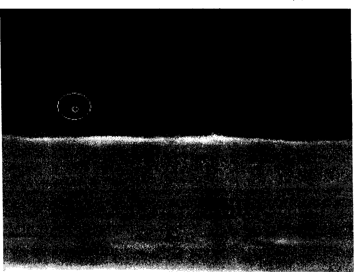
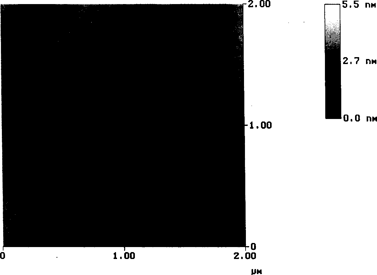
Image

Examples
Embodiment Construction
[0016] The lateral epitaxial growth technique adopted in the present invention comprises the following steps:
[0017] 1. A GaN seed layer is grown on a sapphire substrate by MOCVD, MBE or other methods.
[0018] 2. Deposit SiO on the GaN seed layer 2 、Si 3 N 4 , W and other films as a mask layer, the thickness is 100nm.
[0019] 3. Use photolithography to etch the mask layer to obtain a certain pattern, and the mask area is generally larger than the window area. graphic shape
[0020] There are mainly parallel strips and regular hexagons. For parallel strips, the width of the mask area is 2-20μm, GaN
[0021] The width of the window area is 0.2-20 μm, and the opening direction of parallel strips is along the [1ī00] orientation of GaN. positive six
[0022] Hexagonal openings, so that the [1ī00] orientation of GaN is perpendicular to the sides of the regular hexagon.
[0023] 4. Control the ratio of V-valent N atoms to III-valent Ga atoms (33-83:1), growth te...
PUM
 Abstract
Description
Claims
Application Information
 - R&D
- Intellectual Property
- Life Sciences
- Materials
- Tech Scout
- Unparalleled Data Quality
- Higher Quality Content
- 60% Fewer Hallucinations
Browse by: Latest US Patents, China's latest patents, Technical Efficacy Thesaurus, Application Domain, Technology Topic, Popular Technical Reports.
© 2025 PatSnap. All rights reserved.Legal|Privacy policy|Modern Slavery Act Transparency Statement|Sitemap|About US| Contact US: help@patsnap.com