


Quick Research
Generate reliable direction feasibility study reports for your R&D in just a few steps.

Technical Q&A
Discover and master advanced knowledge NOW. Basics, ideas, possibilities, all at once.

Find Solutions
As an expert in R&D theories, this can generate solutions to your technical problems instantly.

Evaluate Feasibility
Analyze your overall solution with one click, know your potential R&D risks in advance.

Monitor Landscape
Get weekly tech updates, stay abreast of the latest tech innovations and key insights.
Electroluminescent organic device
An electroluminescent device and organic light-emitting layer technology, applied in electroluminescent light sources, electric light sources, electrical components, etc., can solve the problems of reducing the luminous efficiency of the device, unbalanced carrier transmission, etc., to improve the luminous efficiency and luminous Brightness, to achieve the effect of injection balance
- Summary
- Abstract
- Description
- Claims
- Application Information
AI Technical Summary
Problems solved by technology
Method used
Image

Examples
Embodiment 23
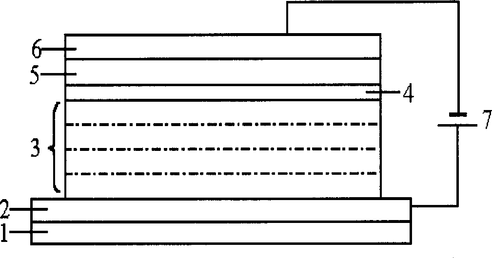
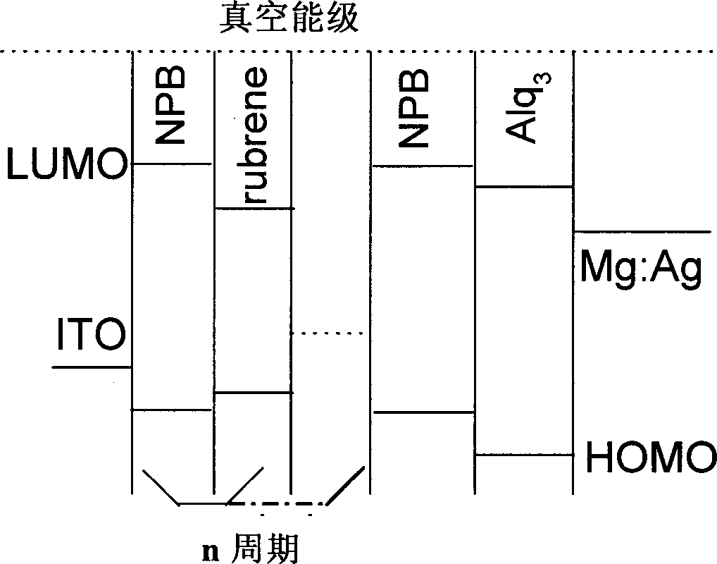
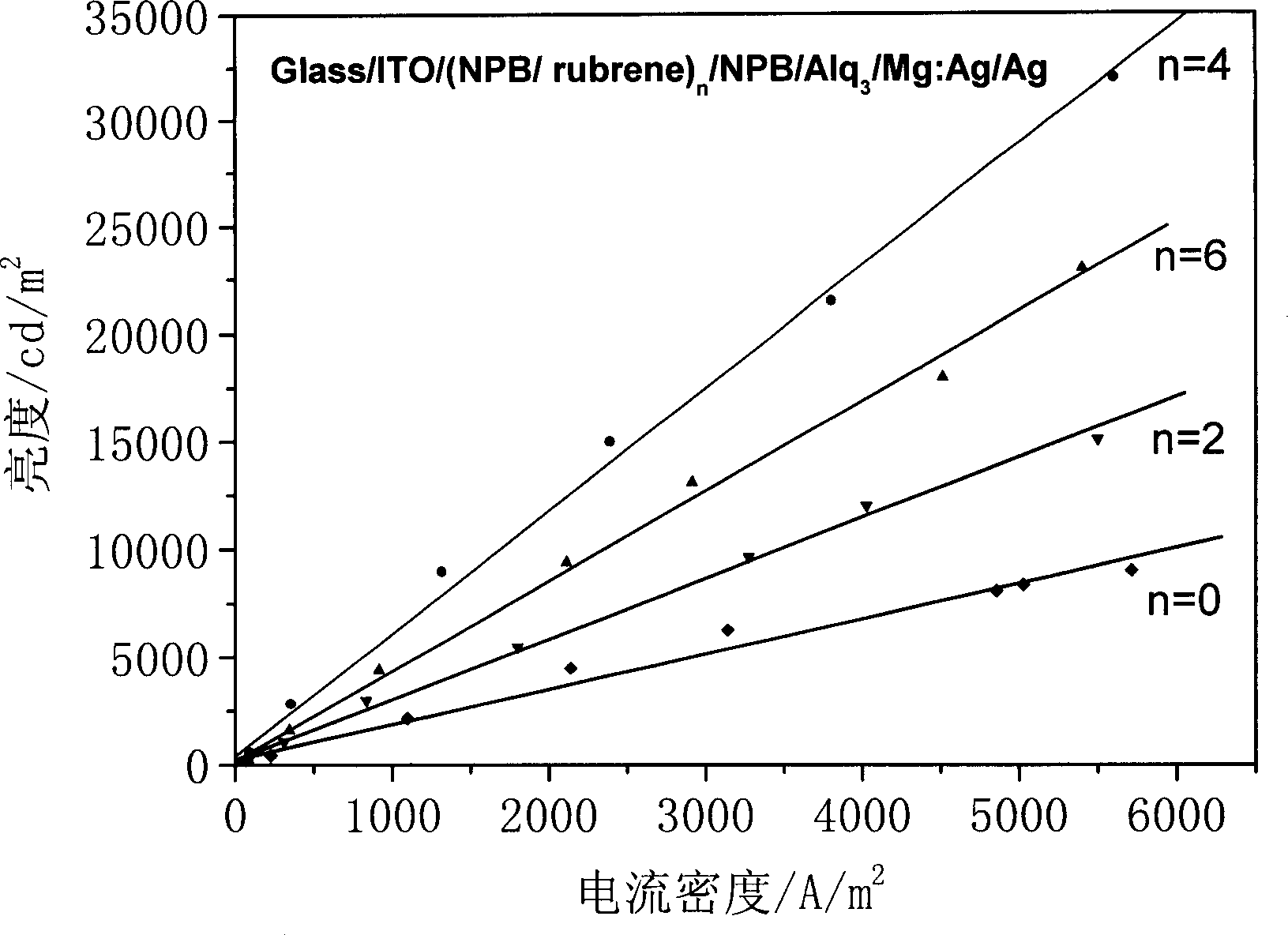
[0048] The ITO glass with a sheet resistance of 15Ω was cleaned and dried by boiling detergent and ultrasonic deionized water, and the film thickness of ITO was 260.0nm. Put the dried ITO glass under a pressure of 1×10 -3 In a vacuum chamber of Pa, a 10.0nm CuPc buffer layer was evaporated on the ITO film by thermal evaporation method, and the evaporation rate was 0.01nm / s. Thereafter, alternate multilayer hole transport layers (NPB / rubrene) are vapor-deposited on top 3 , wherein the evaporation rate of the NPB film is 0.2nm / s, the film thickness is 5.0nm, the evaporation rate of the rubrene film is 0.1nm / s, and the film thickness is 2.0nm. Continue to vapor-deposit a 20.0nm NPB layer on the hole transport layer as a transition layer, the evaporation rate is 0.2nm / s, and continue to evaporate the organic functional layer Al(Saph-q), and the evaporation rate is 0.2nm / s, the film thickness is 60.0nm. On the Al(Saph-q) layer, continue to evaporate the metal layer, the metal l...
Embodiment 24
[0050] The ITO glass with a sheet resistance of 100Ω was cleaned and dried by boiling detergent and ultrasonic waves with deionized water, and the film thickness of ITO was 60.0nm. Put the dried ITO glass under a pressure of 2×10 -3 In a vacuum chamber of Pa, alternate multi-layer hole transport layers (MTDATA / rubrene) are evaporated on the ITO film by thermal evaporation. 10 , where the evaporation rate of the MTDATA film is 0.2nm / s, the film thickness is 5.0nm, the evaporation rate of the rubrene film is 0.1nm / s, and the film thickness is 2.0nm. Continue to vapor-deposit a 5.0nm NPB layer as a transition layer on the hole transport layer, and the evaporation rate is 0.2nm / s, and continue to vapor-deposit an organic functional layer Alq 3 , the evaporation rate is 0.2nm / s, and the film thickness is 60.0nm. in Alq 3 The metal layer is continuously vapor-deposited on the layer, and the metal layer is sequentially composed of Mg:Ag alloy and Ag. The total evaporation rate of ...
Embodiment 25
[0052] The ITO glass with a square resistance of 60Ω was cleaned and dried by boiling detergent and ultrasonic deionized water, and the film thickness of ITO was 100.0nm. Put the dried ITO glass under a pressure of 2×10 -3 In a vacuum chamber of Pa, alternate multi-layer hole transport layers (TPD / DCJTB) were deposited on the ITO film by thermal evaporation. 4 , wherein the evaporation rate of the TPD thin film is 0.2nm / s, the film thickness is 5.0nm, the evaporation rate of the DCJTB thin film is 0.1nm / s, and the film thickness is 2.0nm. Continue to evaporate a 20.0nm TPD layer as a transition layer on the hole transport layer, and the evaporation rate is 0.2nm / s, and continue to evaporate an organic functional layer Alq 3 , the evaporation rate is 0.2nm / s, and the film thickness is 60.0nm. in Alq 3 The metal layer is continuously vapor-deposited on the layer, and the metal layer is sequentially composed of Mg:Ag alloy and Ag. The total evaporation rate of Mg:Ag is 1.5nm / s...
PUM
 Abstract
Description
Claims
Application Information
 - R&D Engineer
- R&D Manager
- IP Professional
- Industry Leading Data Capabilities
- Powerful AI technology
- Patent DNA Extraction
Browse by: Latest US Patents, China's latest patents, Technical Efficacy Thesaurus, Application Domain, Technology Topic, Popular Technical Reports.
© 2024 PatSnap. All rights reserved.Legal|Privacy policy|Modern Slavery Act Transparency Statement|Sitemap|About US| Contact US: help@patsnap.com