Ultraviolet photosensitive device

A technology for photosensitive devices and ultraviolet rays, which is applied to the measurement of ultraviolet rays, electric solid-state devices, semiconductor devices, etc., and can solve problems such as large-scale, band-pass filter degradation, and cost increase

Inactive Publication Date: 2003-06-11
FUJIFILM BUSINESS INNOVATION CORP
View PDF0 Cites 3 Cited by
  • Summary
  • Abstract
  • Description
  • Claims
  • Application Information

AI Technical Summary

Problems solved by technology

For this reason, the structure of the ultraviolet detection sensor will be complicated and enlarged, and the cost will also be increased.
Furthermore, because the light passing through the band-pass filter or waveguide channel is incident on the ultraviolet photosensitive device, its light sensitivity will be reduced.
In addition, since the bandpass filter will be degraded by ultraviolet rays, the ultraviolet photosensitive device will also have the problem of deterioration

Method used


Image

  • Ultraviolet photosensitive device
  • Ultraviolet photosensitive device
  • Ultraviolet photosensitive device

Examples


example 1

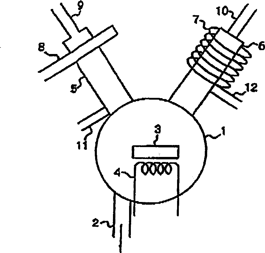
[0118] A cleaned quartz substrate (thickness: 0.2 mm, length: 10 mm, width: 10 mm) was placed on the substrate holder 3 . Then, use a rotary pump and a mechanical booster turbo pump connected to the exhaust port 2 to vacuum exhaust the reaction chamber 1 so that its back pressure is lower than 10 -3 Pa, the above-mentioned quartz substrate is heated to about 500 degrees Celsius by the heater 4 .

[0119] Afterwards, the nitrogen gas of 1000 sccm (standard cubic centimeter per miniutue) is introduced into the quartz tube 5 with a diameter of 25 mm through the gas introduction pipe 9, and the output power of the microwave at 45 GHz is adjusted to 250 W by the regulator, and then passed through the microwave conduit 8 to discharge. The reflected wave at this time was 0W. Furthermore, 1 sccm means that at 1013.25 hPa (1 atmospheric pressure) and 0 degrees Celsius, the flow rate of gas is equivalent to 1 cubic centimeter per minute.

[0120]Furthermore, 500 sccm of hydrogen gas ...

example 2

[0138] Except that when forming the first electrode layer, only trimethylaluminum, which is the raw material of group IIIA elements, is introduced into the gas introduction tube 11 under the same conditions as in Example 1, all the others are carried out under the same conditions as in Example 1. Formation of an electrode layer.

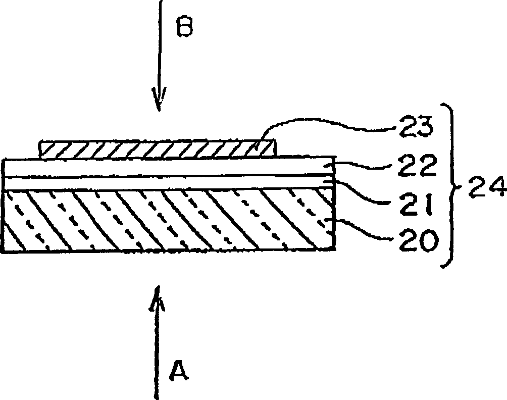
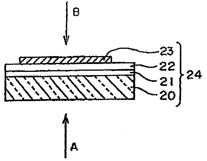
[0139] Thus, on the surface of the quartz substrate, a silicon-doped AlN:H film with a film thickness of 100 nm was formed as a first electrode layer. In addition, the hydrogen content in the film measured by the IR method (infrared spectroscopic analysis method) was 5 atomic %.

[0140] Then, after the film-forming chamber 1 returns to atmospheric pressure, the quartz substrate on which the first electrode layer has been formed is taken out from the film-forming chamber 1, and the end of the first electrode layer is covered with a metal mask, and then the aforementioned substrate is formed with the first electrode layer. An electrode layer is place...


PUM


Abstract

Providing a UV optical device with which UV in a desired wavelength region can be detected without using a band-pass filter and a waveguide, featuring less dependence on the angle of incidence, high photosensitivity, simple constitution, and enabling assembly of a stable and accurate UV detector at a low cost. The UV photo-detector comprises at least a 1st electrode layer, and a sensor layer. The 1st electrode layer comprises a semiconductor containing at least one element selected from a group of Al, Ga, and In, and nitrogen or oxygen. The sensor layer comprises a semiconductor containing at least one element selected from a group of Al, Ga, and In, and nitrogen. A long wavelength absorption edge of the 1st electrode layer is closer to the side of the short wavelength than the long wavelength absorption edge of the sensor layer.

Description

technical field [0001] The present invention relates to an ultraviolet photosensitive device. Background technique [0002] In recent years, among the environmental problems on the earth, one of the major problems is the increase in the amount of ultraviolet rays on the earth's surface due to the destruction of the ozone layer. In particular, the increase in the amount of ultraviolet rays with a wavelength of 330 nm or less on the ground surface becomes more remarkable due to the reduction of ozone in the ozone layer. [0003] Due to the increase of ultraviolet rays, there will be significant impacts on human health, such as the occurrence of skin cancer, the increase of photosensitivity caused by DNA damage, and photoaging. For example, high-energy ultraviolet rays in a short-wavelength range of 320 nm or less called UV-B are known to cause various damages to the skin by causing damage to DNA. Furthermore, ultraviolet rays in a long wavelength range above 320nm, called UV...

Claims


Application Information

Patent Timeline
Patent Type & Authority Applications(China)
IPC IPC(8): H01L31/10G01J3/28H01L27/14H01L31/00H01L31/0232H01L31/075H01L31/09H01L31/107
CPCG01J1/429H01L31/1852H01L31/09H01L31/109Y02E10/544H01L31/0304H01L31/022408Y02E10/548Y02P70/50
Inventor 八木茂
Owner FUJIFILM BUSINESS INNOVATION CORP
Why Eureka
Try Eureka