Transparent metal dielectric composite material

A technology of composite materials and transparent metals, applied in the direction of conductive materials, conductive materials, circuits, etc., can solve the problems of peak transmittance decrease, high transmittance area narrowing, etc.

Inactive Publication Date: 2003-06-25
张会琴 +1
View PDF0 Cites 13 Cited by
  • Summary
  • Abstract
  • Description
  • Claims
  • Application Information

AI Technical Summary

Problems solved by technology

When the number of metal layers is kept constant and the thickness of each layer of metal is increased, or the number of metal layers is increased while the thickness of each layer of metal is kept constant, so that the total thickness of the metal film increases, the corresponding improvement of the infrared or microwave blocking ability, but The high transmittance area of ​​the material in the visible range will be significantly narrowed, and the peak transmittance will be significantly reduced

Method used


Image

  • Transparent metal dielectric composite material
  • Transparent metal dielectric composite material
  • Transparent metal dielectric composite material

Examples


Embodiment Construction

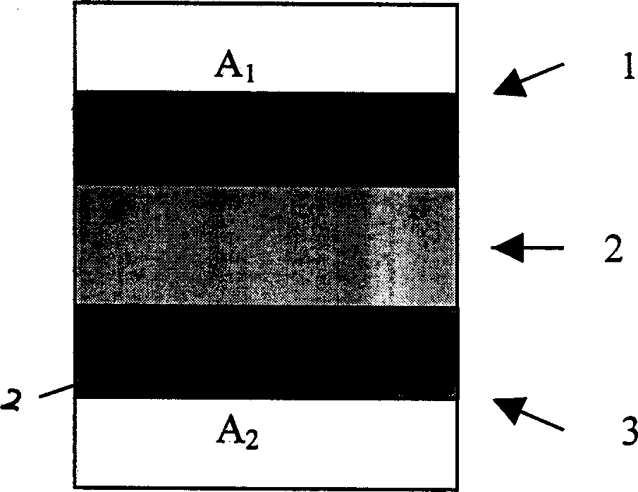
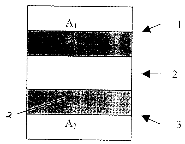
[0008] Such as figure 1 As shown, the preferred mode of realizing the present invention is: the transparent metal-dielectric composite material of a kind of semiconductor quantum well structure of the present invention is made of induction layer 1,3 and functional layer 2, and described induction layer 1,3 is made of two layers respectively Transparent Dielectric Film A 1 , B 1 and B 2 、A 2 Composition, the functional layer 2 is made of metal material, the functional layer 2 is compounded between the induction layers 1 and 3, the thickness of the functional layer 2 is between 3 nanometers and 9000 nanometers, the functional layer as a single-layer metal film. Such as figure 2 As shown, the functional layer 2 may also be composed of multiple layers of metal films and dielectric films. The method of electron beam evaporation or sputtering in the prior art may be used to combine the functional layer with the inductive layer. In a preferred embodiment of the present invent...


PUM

PropertyMeasurementUnit
thicknessaaaaaaaaaa
thicknessaaaaaaaaaa
thicknessaaaaaaaaaa

Abstract

The transparent composite metal dielectric material consists of two inducing layers and one functional layer between the two inducing layers and features that each inducing layer consists of two layers of different transparent dielectric film and the two inducing layers may have different optical thickness. The function layer may have doped inducing layer material to form multiple quantum well structure. By means of multiple reflection and quantum well-like resonant effect, the composite material anti-reflects the electromagnetic wave in required wave band while reflecting electromagnetic waves of other wavelengths. The present invention may be used as windoe material or transparent body material a well as in producing metal semiconductor photoelectronic detector and other relevant device.

Description

Technical field: [0001] The invention relates to a composite film material or device for electromagnetic wave signal processing, in particular to a transparent metal dielectric composite material with a symmetrical structure similar to semiconductor quantum wells. Background technique: [0002] In the prior art, devices usually used for electromagnetic wave signal (optical signal) processing are all-optical devices or optoelectronic devices mixed with optical and electronic devices, and are mostly made of dielectric materials, semiconductor materials, and the like. Electromagnetic wave signals are divided by wavelength from short to long, including gamma rays, X-rays, ultraviolet, visible light bands, infrared, microwave, radio waves, long waves, etc. With the development of the information age, the processing of photoelectric signals is moving towards broadband and high-speed The development of the corresponding direction puts forward higher requirements for the devices and...

Claims


Application Information

Patent Timeline
Patent Type & Authority Applications(China)
IPC IPC(8): B32B5/00B82B1/00C09K3/00G02B1/00H01B1/00H01B3/00H01L31/0224
CPCH01L31/022466B82Y10/00
Inventor 张会琴潘晓英
Owner 张会琴
Why Eureka
Try Eureka