Blue light emitting device of III group nitrogen semi-conductor

A technology of nitride semiconductors and light-emitting devices, which is applied in semiconductor devices, electrical components, circuits, etc., can solve the problems of large lattice mismatch, high defect density of epitaxial layers, and low mobility, so as to reduce scattering and improve electrical properties , the effect of improving the migration rate

Inactive Publication Date: 2003-07-23
SOUTH CHINA NORMAL UNIVERSITY
View PDF0 Cites 29 Cited by
  • Summary
  • Abstract
  • Description
  • Claims
  • Application Information

AI Technical Summary

Problems solved by technology

However, due to the very large lattice mismatch between sapphire (a=4.758) and GaN (a=3.189), the epitaxial layer has a large defect density and low mobility

Method used


Image

  • Blue light emitting device of III group nitrogen semi-conductor
  • Blue light emitting device of III group nitrogen semi-conductor
  • Blue light emitting device of III group nitrogen semi-conductor

Examples


Embodiment Construction

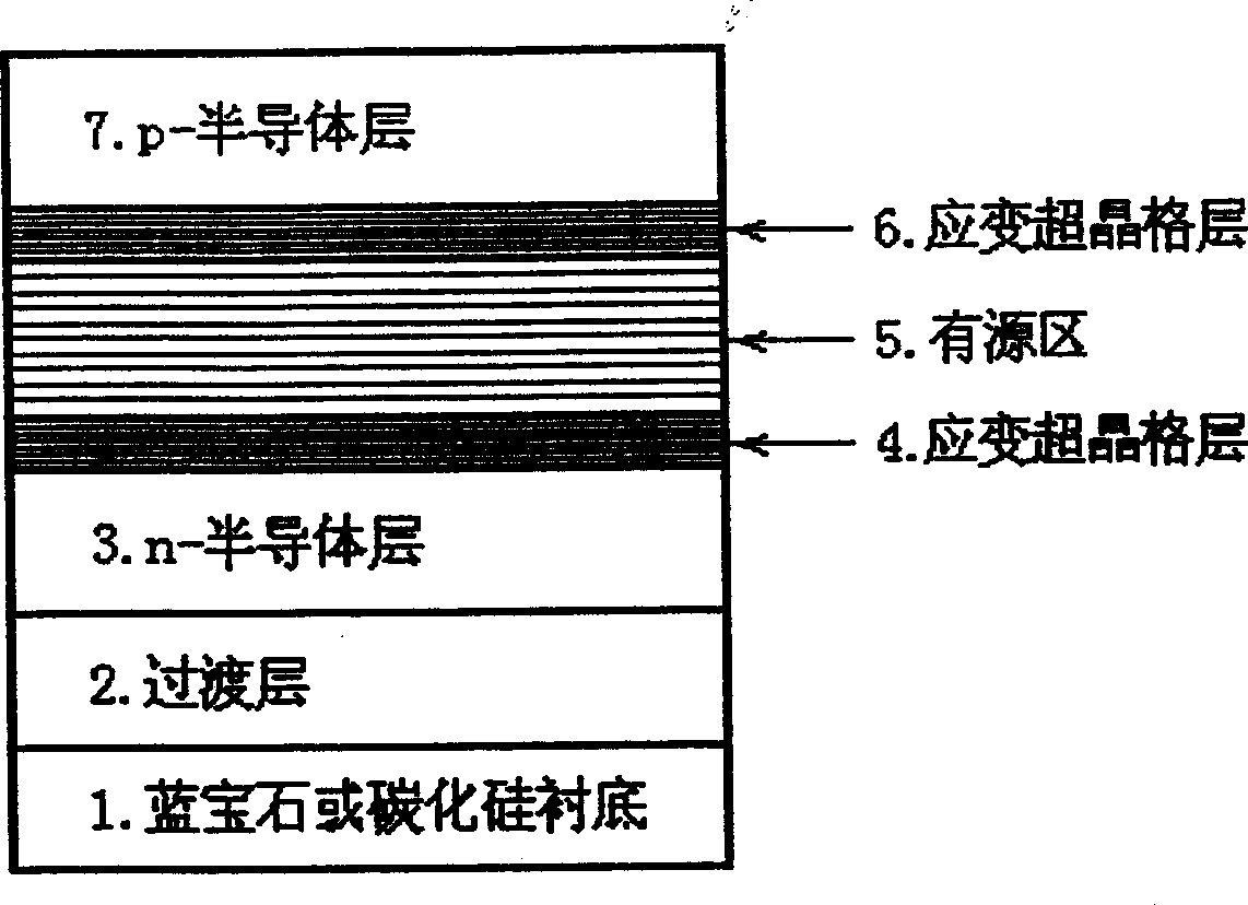
[0021] Such as figure 1 As shown, in α-Al 2 o 3 Undoped GaN2, n-type GaN3, n-type strained layer superlattice 4, InGaN / GaN multiple quantum wells 5, p-type strained layer superlattice 6 and p-type GaN7 are sequentially grown on the substrate 1.

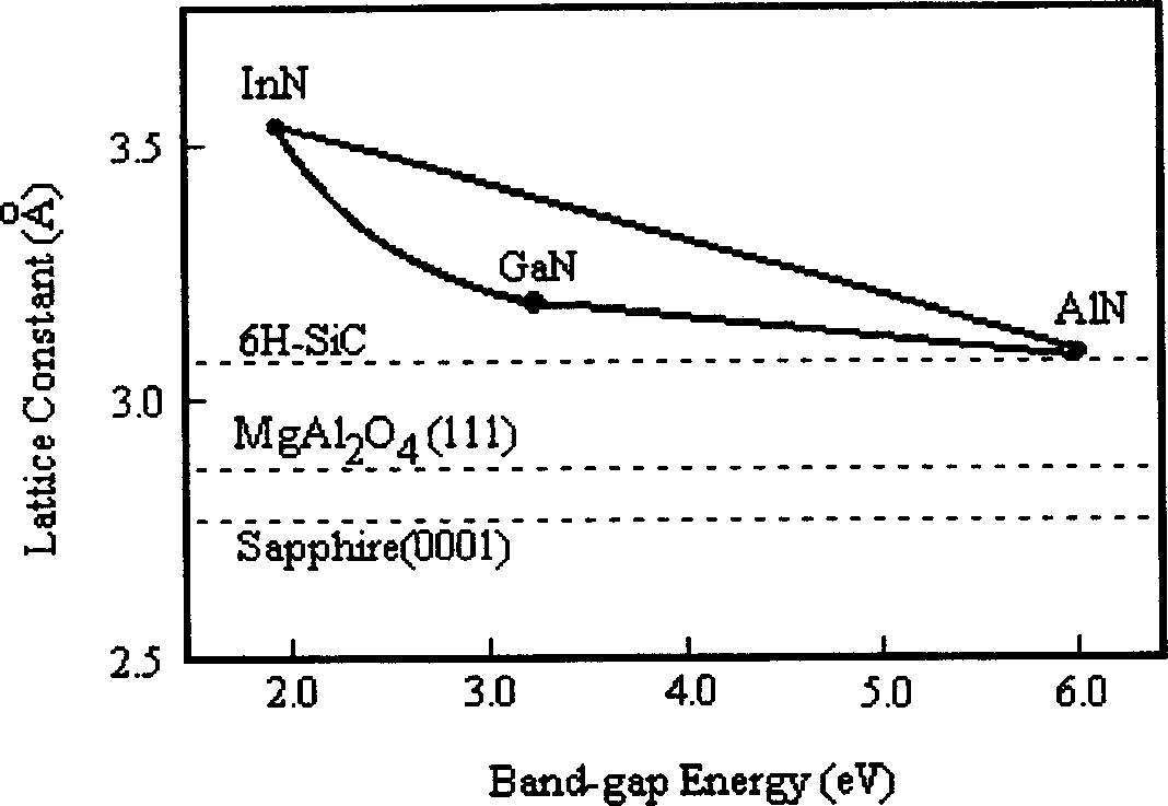
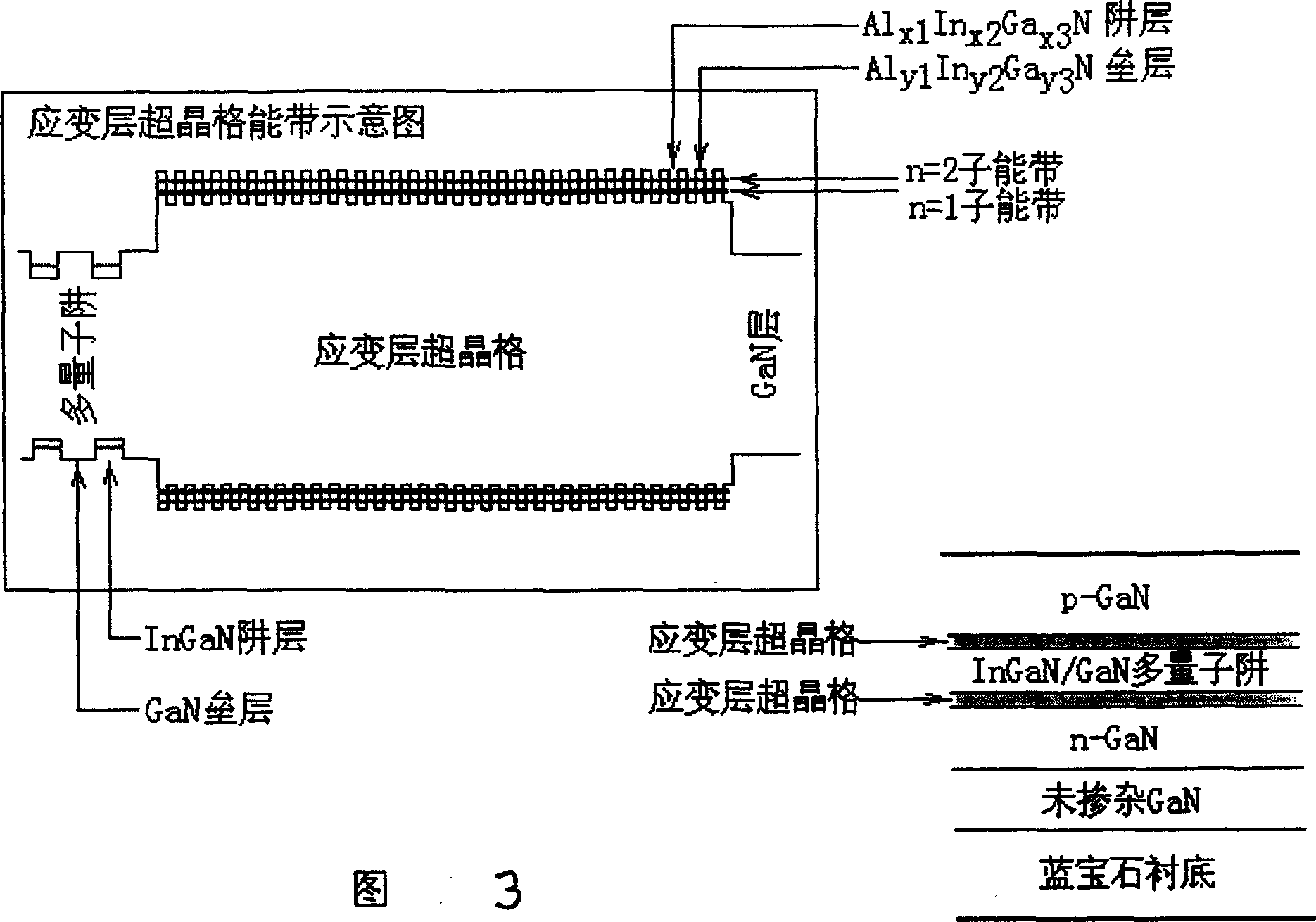
[0022] Such as figure 2 As shown, it represents III-V semiconductor materials GaN, InN, AlN and substrate materials 6H-SiC, MgAl 2 o 4 (111), α-Al 2 o 3 The lattice constant and energy band gap. It can be seen that the lattice constant of InN is larger than GaN, and the band gap is smaller than GaN; while the lattice constant of AlN is smaller than and close to GaN, and the band gap is much larger than GaN. Therefore, the M shown in Figure 3 can be selected * (Al x1 In x2 Ga x3 N-Al y1 In y2 Ga y3 N) Strained layer superlattice as cladding. At this time, y2 takes zero or a smaller value, Al y1 In y2 Ga y3 The lattice constant of the N barrier layer is similar to that of the usual AlGaN cladding layer, and slightly s...


PUM


Abstract

The invention relates to the blue light-emitting device of III group nitrogen semi-conductor. Clads on the two sides of the active area includes at least one strained layer superlattice structure. Comparing with general AIGaN clad, the structure can eliminate the defect caused by the mismatch between GaN and the crystal lattice of the substrate so as to improve the crystal perfection and confine carriers in the active area effectively and uniformly. Thus, the combined luminous efficiency and the uniformity are raised.

Description

technical field [0001] The invention relates to a semiconductor device, in particular to a group III nitride semiconductor blue light-emitting device. Background technique [0002] For optoelectronic devices such as light-emitting diodes and semiconductor lasers, it is required that the injected electrons (n-type carriers) and holes (p-type carriers) can be confined to the active layer (active layer), where they recombine and emit light. . On both sides of the active region, a semiconductor material with a larger forbidden band width than the active layer is used to form a barrier layer, and according to the difference in doping, the confinement of electrons and holes can be achieved respectively. For cladding materials, not only the ability to form an appropriate barrier height must be considered. It is also necessary to consider whether it can lattice match with the semiconductor layers and active layers on both sides, otherwise it will destroy the structure and performa...

Claims


Application Information

Patent Timeline
Patent Type & Authority Applications(China)
IPC IPC(8): H01L33/06H01S5/30
Inventor 范广涵
Owner SOUTH CHINA NORMAL UNIVERSITY
Why Eureka
Try Eureka