NEMS piezoresistive pressure sensor chip and its making process

A pressure sensor and piezoresistive technology, which is applied in the field of MEMS devices, can solve the problems of poor uniformity of pressure-sensitive film thickness, poor piezoresistive consistency, and difficult leakage current, so as to improve yield, reduce leakage current, and reduce zero point output effect

Inactive Publication Date: 2003-07-30
PEKING UNIV
View PDF0 Cites 27 Cited by
  • Summary
  • Abstract
  • Description
  • Claims
  • Application Information

AI Technical Summary

Problems solved by technology

However, although the piezoresistive sensor has already formed a product, the MEMS piezoresistive chip as its core has limited the application of the MEMS piezoresistive pressure sensor

Method used


Image

  • NEMS piezoresistive pressure sensor chip and its making process
  • NEMS piezoresistive pressure sensor chip and its making process
  • NEMS piezoresistive pressure sensor chip and its making process

Examples


Embodiment Construction

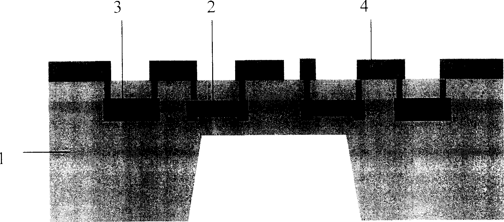
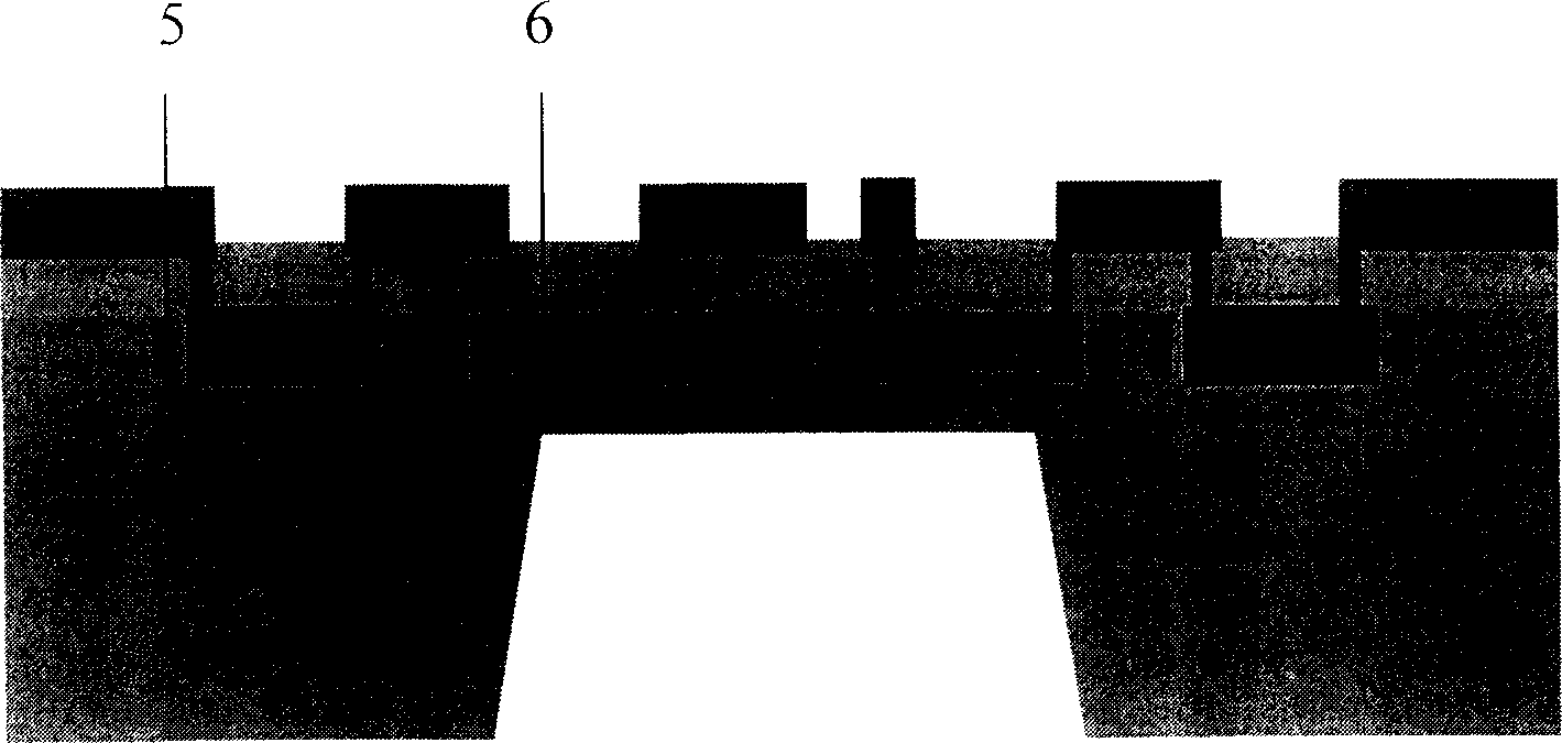
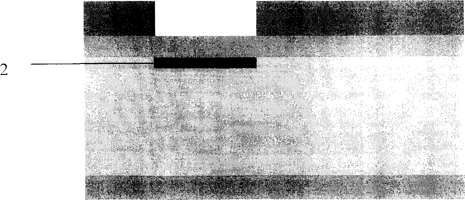
[0023] A 4-inch 400-micron-thick N-type double-sided polished single crystal silicon wafer is used, with a resistivity of 2-4Ωcm.

[0024] 1. After the silicon wafer is cleaned, perform original oxidation of 300-350nm;

[0025] 2. The high-precision piezoresistor is prepared by ion implantation technology, and the implantation conditions are: 90-120KeV, 1.0×10 14 cm -2 -2.0×10 14 cm -2 , and then carry out boron drive-in, the condition is 1000-1500 ℃, 80-120 minutes;

[0026] 3. Diffusion of concentrated phosphorus forms n + Isolation, body concentration > 1.0×10 after annealing 19 cm -3 ;

[0027] 4. Concentrated boron diffuses to form p + Connection, body concentration > 5.0×10 after annealing 18 cm -3 ;

[0028] 5. KOH corrodes the back cavity, and the thickness of the film is controlled by the mark on the front of the pressure-sensitive film;

[0029] 6. Engraving lead holes, sputtering aluminum, alloy, 400-420°C, 30 minutes;

[0030] 7. Bonding, dicing, fina...


PUM


Abstract

The MEMS piezoresistive pressure sensor chip is one cup-shaped structure including one squared pressure-sensing film, peripheral support and four piezoresistors, which are in the maximum strain area of the pressure-sensing film constitute point bridge to sense pressure change. The piezoresistors are made by ion implantation technology and there is a circle of n+isolating area around each piezoresistor and aligning mark in the edge of the pressure-sensing film to monitor the thickness of the pressure-sensing film. Compared with conventional diffusion technology, the ion implantation technologyhas higher piezoresistor precision, lower zero input and lower zero temperature drift. The increased n+isolating area raises the long-term stability of chip, and the aligning mark makes the etching of the sensing film more controllable.

Description

Technical field: [0001] The invention relates to a MEMS (micro-electro-mechanical system) device, in particular to a MEMS piezoresistive pressure sensor chip. Background technique: [0002] Micro electromechanical systems (Micro electro mechanical Systems-American idiomatic words), also known as micromachines (Micromachine-Japanese idiomatic words) and microsystems (Microsystems-European idiomatic words), refer to micro-mechanical processing technology including microsensors, Micro-electromechanical devices and devices composed of micro-mechanical basic parts such as micro-actuators and micro-energy sources, and high-performance electronic integrated circuits. Micro-electromechanical systems with micro-mechanics as the research object involve a variety of disciplines, mainly including basic content such as micro-mechanics, microelectronics, automatic control, physics, chemistry, biology, and material science. It is a multi-disciplinary, high-tech marginal discipline. . To ...

Claims


Application Information

Patent Timeline
IPC IPC(8): G01L9/06
Inventor 张威张大成刘蓓李婷王阳元
Owner PEKING UNIV
Why Eureka
Try Eureka