
Eureka
For R&D, Eureka makes reading and utilizing patents & technical documents easy.
Eureka AIR
Designed for self-driven R&D workflows. Generate viable solutions, solve complex R&D challenges, empower your innovation with AI.

Eureka Materials
Designed for material experts only. Revolutionize your material R&D, from search, analyze, to developing new materials.

TechResearch
Generate reliable direction feasibility study reports for your R&D in just a few steps.

TechSeek
Discover and master advanced knowledge NOW. Basics, ideas, possibilities, all at once.

TechMind
As an expert in R&D Theories, TechMind can generates customized viable solutions instantly.

TechRisk
Analyze your overall solution with one click, know your potential R&D risks in advance.

TechMonitor
Get weekly tech updates, stay abreast of the latest tech innovations and key insights.
Mfg. method of semiconductor device
A manufacturing method and semiconductor technology, applied in semiconductor/solid-state device manufacturing, manufacturing tools, grinding devices, etc., can solve problems such as weak mechanical strength and increased CMP frictional resistance
- Summary
- Abstract
- Description
- Claims
- Application Information
AI Technical Summary
Problems solved by technology
Method used
Image

Examples
Embodiment 1
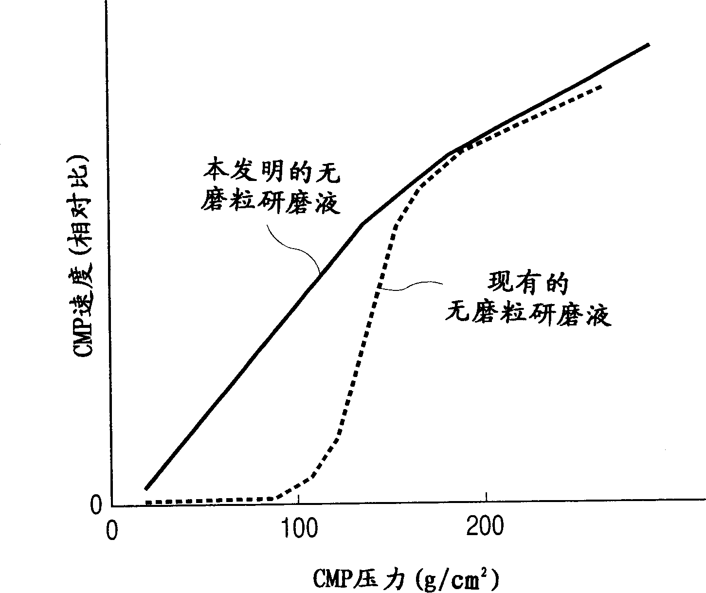
[0072] The difference in characteristics between the abrasive-free polishing liquid according to the present invention and the conventional abrasive-free polishing liquid will be described focusing on polishing characteristics. As the abrasive-free grinding liquid of the present invention, as the first corrosion agent, it contains 0.15% by volume of phosphoric acid, as the second corrosion agent, it contains 0.6 volume% of lactic acid, as the first corrosion inhibitor, it contains 0.2% by weight of BTA, as The second anticorrosion agent contains 0.4% by weight of imidazole, and contains 0.05% by volume of polyacrylic acid neutralized with ammonia, hydrogen peroxide (H 2 o 2 Concentration 30% by weight) 30% by volume, the rest is deionized water. Here, when the raw material is solid, it is represented by weight%, and when it is liquid, it is represented by volume%. As the substrate to be polished, thermally oxidized SiO is formed on the surface 2 On a 4-inch silicon wafer, a...
Embodiment 2
[0079] In this example, the case of performing CMP on a copper or copper-based alloy film on a large-area substrate to be polished using the same polishing solution as in Example 1 will be described. As a substrate to be polished, an 8-inch-diameter silicon wafer was used. Form 50nm thick SiO on its surface by thermal oxidation 2 A film on which tantalum and copper or an alloy film mainly composed of copper is formed with a thickness of 50 nm and 1 μm by a known sputtering method. Then, CMP of copper or an alloy mainly composed of copper was performed under the same conditions as in Example 1. However, the flow rate of the polishing liquid was 300 ml / min. The same CMP speed was obtained for a small 4 inch diameter substrate, about 460 nm / min. In this example, it is worth noting that the in-plane distribution of the CMP rate is a very small value of ±5% or less regardless of the use of an 8-inch large-area wafer.
Embodiment 3
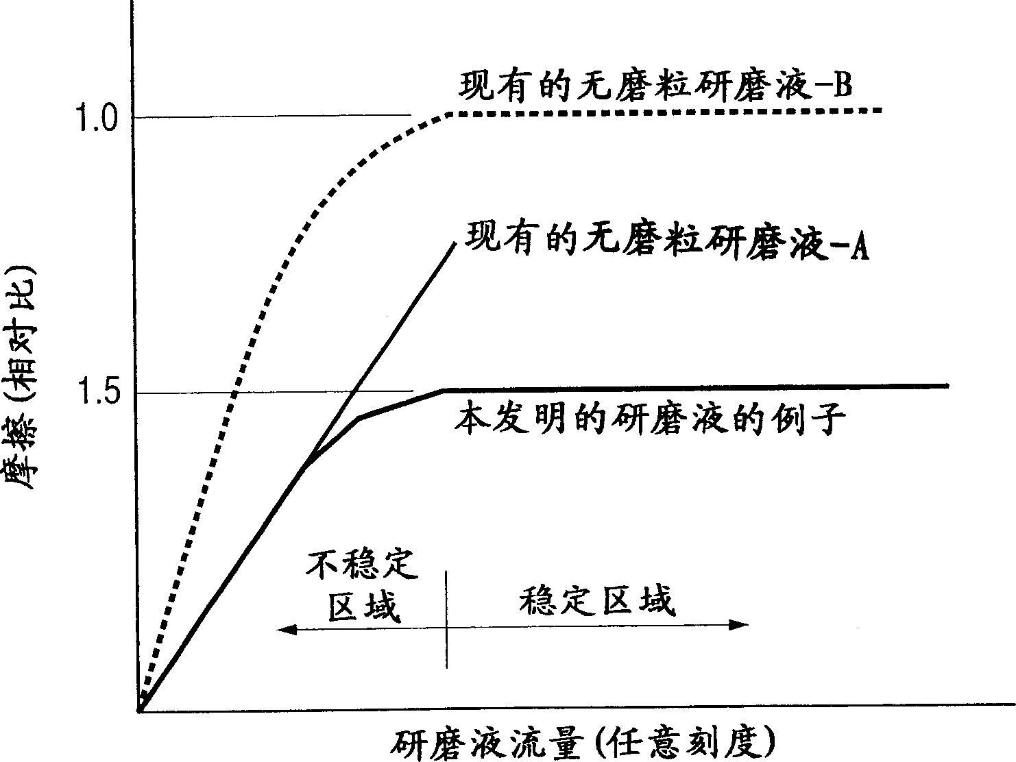
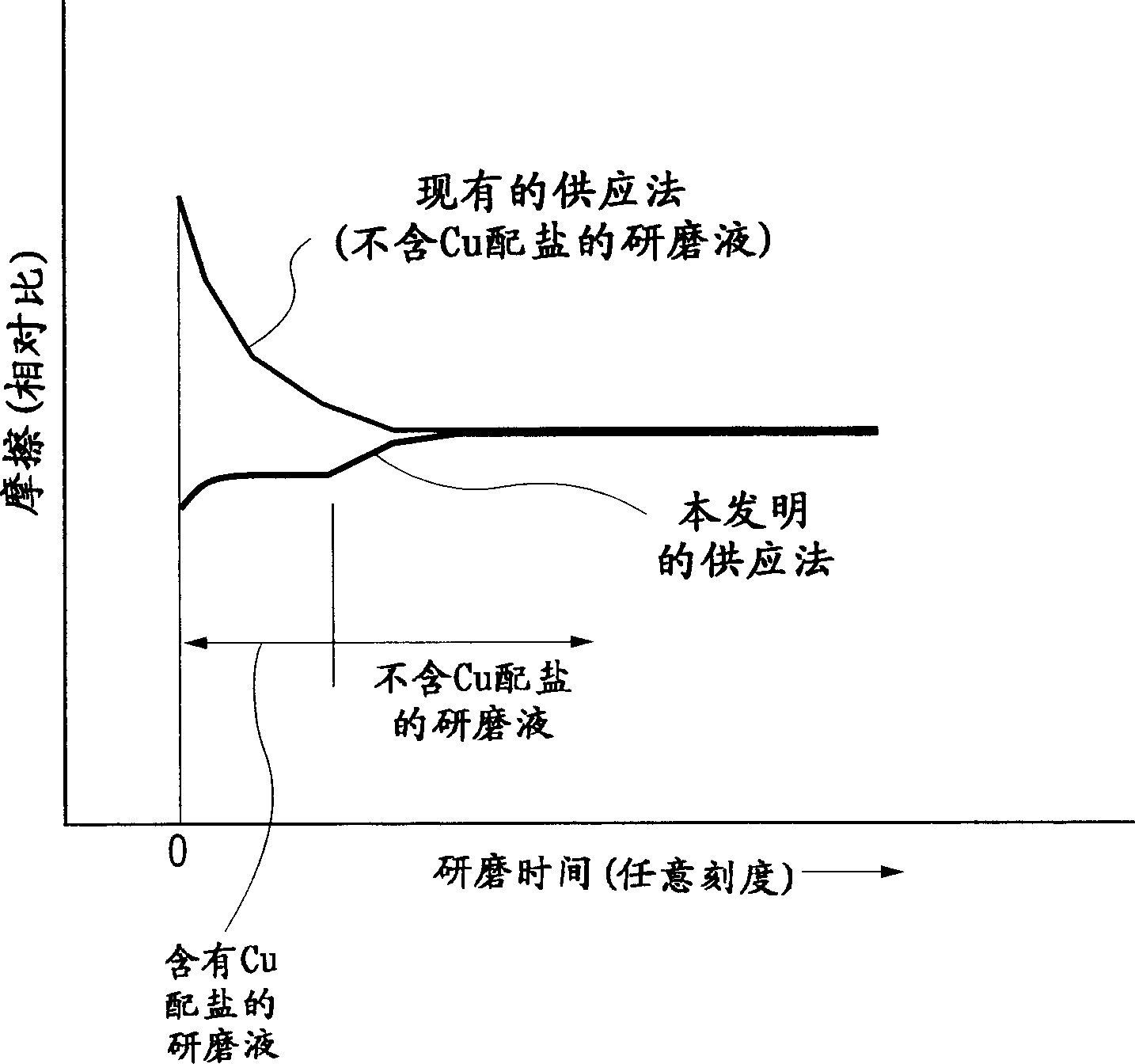
[0082] In this example, an example of a polishing liquid in which copper or a complex salt of an alloy mainly composed of copper is further added to the polishing liquid of the present invention is shown. Except grinding liquid, others are identical with embodiment 1. In the above embodiment, if the abrasive-free polishing liquid of the present invention is used, the friction caused by the existing abrasive-free polishing liquid can be reduced by 1 / 2. However, the absolute value of friction does not always remain at 60g / cm throughout the CMP process 2 the following.
[0083] In the description of the previous Example 1 figure 1 Among them, the reason why the friction decreases when the flow rate of the polishing liquid is small is as follows. In CMP of copper or an alloy mainly composed of copper, a large amount of reaction products are generated. The reaction product is a complex salt formed by the reaction of copper or an alloy mainly composed of copper and a corrosive ...
PUM
| Property | Measurement | Unit |
|---|---|---|
| thickness | aaaaa | aaaaa |
| thickness | aaaaa | aaaaa |
| diameter | aaaaa | aaaaa |
Abstract
Description
Claims
Application Information
 - R&D Engineer
- R&D Manager
- IP Professional
- Industry Leading Data Capabilities
- Powerful AI technology
- Patent DNA Extraction
Browse by: Latest US Patents, China's latest patents, Technical Efficacy Thesaurus, Application Domain, Technology Topic, Popular Technical Reports.
© 2024 PatSnap. All rights reserved.Legal|Privacy policy|Modern Slavery Act Transparency Statement|Sitemap|About US| Contact US: help@patsnap.com