Horizontal epitaxial growth of gallium nitride and its compound semiconductor

A technology of lateral epitaxial growth and gallium nitride, which is applied in the field of lateral epitaxial growth of gallium nitride and its compound semiconductors, can solve the problems of prolonging the epitaxial growth time, increasing the cost, affecting the fabrication of devices, etc.

Inactive Publication Date: 2004-04-21
INST OF SEMICONDUCTORS - CHINESE ACAD OF SCI
View PDF0 Cites 41 Cited by
  • Summary
  • Abstract
  • Description
  • Claims
  • Application Information

AI Technical Summary

Problems solved by technology

However, the 90-degree turn of the threading dislocation and the contact stress between the laterally grown GaN and the mask region will cause the laterally grown GaN to have a crystal plane tilt, that is, the GaN (0001) crystal plane of the laterally grown region is aligned with the mask region. The GaN (0001) crystal planes grown in the window region have a crystal plane orientation difference in the direction perpendicular to the mask strip
The existence of misorientation will cause great difficulty in the subsequent merging of adjacent GaN strips, which will produce inclined grain boundaries at the merging and cause undulations on the sample surface
In order to solve this problem, it is generally used to reduce the lateral growth rate, so that the samples are only merged when they are very thick, which greatly prolongs the epitaxial growth time and increases the cost of growth. Causes cracking of the GaN layer, which directly affects subsequent device fabrication

Method used


Image

  • Horizontal epitaxial growth of gallium nitride and its compound semiconductor
  • Horizontal epitaxial growth of gallium nitride and its compound semiconductor
  • Horizontal epitaxial growth of gallium nitride and its compound semiconductor

Examples


specific Embodiment

[0020] Specific examples (see Figure 4 ):

[0021] 1. First, a layer of intrinsic GaN 41 is deposited on a sapphire (0001) substrate 40 by MOCVD, and the thickness of the intrinsic GaN layer is 2 μm.

[0022] 2. Deposit a layer of SiN on the surface of GaN by PECVD x 42 is used as a mask area, and the thickness of the mask area is 0.03 μm.

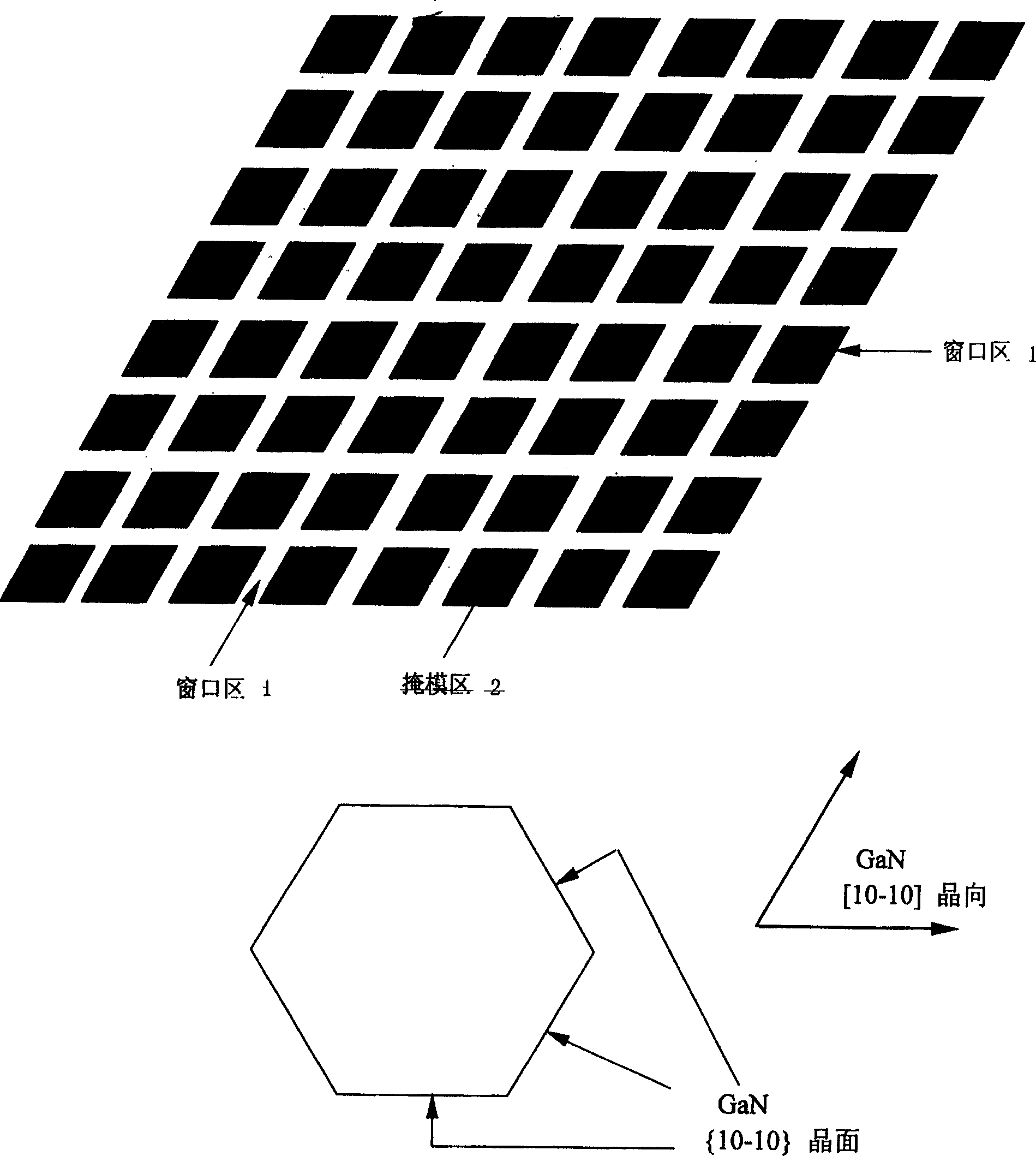
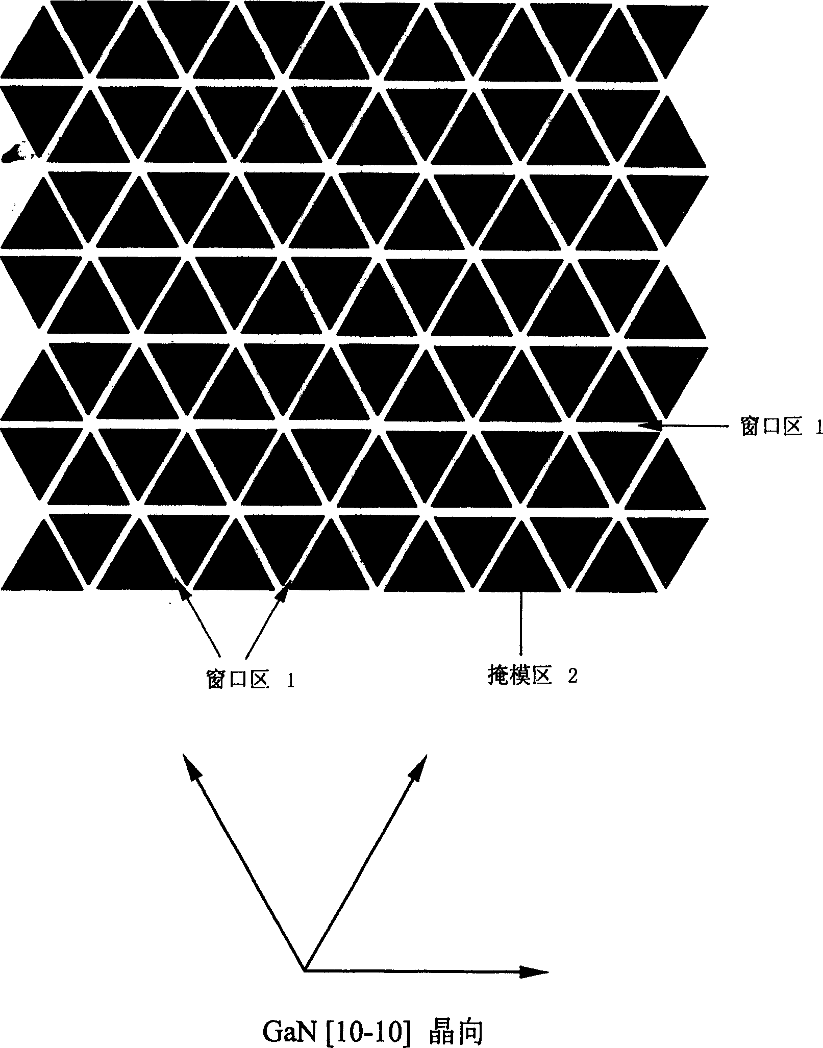
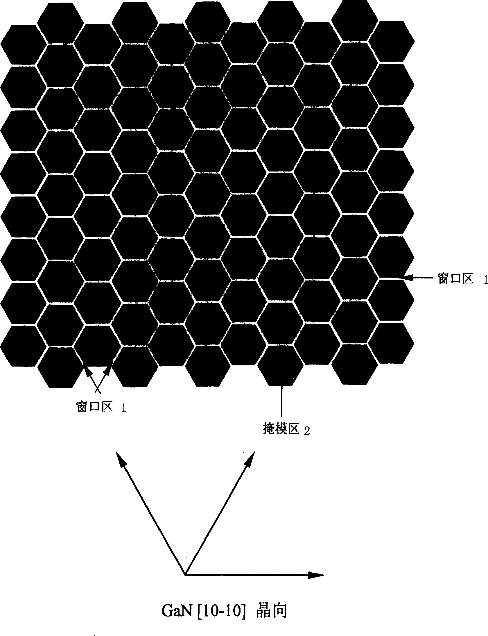
[0023] 3. Using photolithography and wet etching process on SiN x 42 The pattern is engraved on the mask area, and the pattern of the mask area is designed as a rhombic structure with the [10-10] crystal orientation of GaN on the edge of the adjacent window, and the included angle is 60 degrees or 120 degrees. The window area width is 4 μm, and the diamond mask The side length of the mold area is 12 μm.

[0024] 4. Secondary epitaxial growth of GaN and its compound semiconductor 43 is performed on the GaN 41 with a rhombic mask area by MOCVD.

[0025] Depend on Figure 5 It can be seen that the lateral epitaxial GaN surface obtained...


PUM

PropertyMeasurementUnit
thicknessaaaaaaaaaa
thicknessaaaaaaaaaa
thicknessaaaaaaaaaa

Abstract

The present invention provides a method for growing a lateral epitaxy of the gallium nitride and its compound semiconductors, comprising the following steps: growing an intrinsic gallium nitride on the ( 0001 ) crystal face of sapphire or the ( 111 ) of silicon or the ( 0001 ) of silicon carbide using the metal organic chemical vapor deposition or the molecule beam epitaxy or the hydride vapor epitaxy; then depositing on it a layer of silicon nitride or silicon dioxide or silicon nitride-oxide as the mask area; patterning the mask area using the photolithography and wet or dry etch techniques, the pattern of the mask area being designed into the pattern structure of the triangle or parallelogram or rhombus or hexagon with the included angles of 60 or 120 degrees or the combination of above shapes which are constituted of the [ 10 - 10 ] crystal direction of gallium nitride on the edge of the adjacent windows; and finally growing the secondary epitaxy, that is, lateral epitaxy of gallium nitride and its compound using the metal organic vapor deposition or the molecule beam epitaxy or the hydride vapor epitaxy.

Description

technical field [0001] The invention belongs to the technical field of semiconductors, in particular to a lateral epitaxial growth method of gallium nitride and compound semiconductors thereof. Background technique [0002] Group III-V gallium nitride (GaN) and its compound semiconductors, as typical representatives of the third-generation semiconductor materials, have great application prospects in the fields of optoelectronics and microelectronics due to their unique physical, chemical and mechanical properties. However, due to the difficulty in preparing GaN bulk single crystals and the lack of matching heterogeneous substrate materials, GaN is mainly used on large mismatch substrates (Al2O3 (Al 2 o 3 ), with a mismatch of 16%; silicon (Si), with a mismatch of 17%; silicon carbide (SiC), with a mismatch of 3.4%) for epitaxial growth, misfit dislocations and threading dislocations in the epitaxial GaN layer Equal defect densities up to 10 10 ~10 11 cm -2 . These defe...

Claims


Application Information

Patent Timeline
Patent Type & Authority Applications(China)
IPC IPC(8): H01L21/20H01L21/205
Inventor 冯淦杨辉梁骏吾
Owner INST OF SEMICONDUCTORS - CHINESE ACAD OF SCI
Why Eureka
Try Eureka