Mfg. method of assembly set with electronic component and mfg. method for related products

A technology of electronic components and manufacturing methods, which is applied to the direction of assembling printed circuits containing printed electrical components, electrical components, electrical components, etc., which can solve problems such as low productivity, short circuit, poor contact, etc., achieve high productivity and reduce damage , powerful effect

Inactive Publication Date: 2004-05-26
PANASONIC CORP
View PDF0 Cites 3 Cited by
  • Summary
  • Abstract
  • Description
  • Claims
  • Application Information

AI Technical Summary

Problems solved by technology

Therefore, the number of electronic components that can be mounted on one motherboard 11 and the area for forming circuit patterns depend on the size of the motherboard 11, thus failing to meet the recent need to minimize the motherboard 11.
[0011] Moreover, since the semiconductor element 1 and the solder paste 7 are directly exposed to the air, oxidation will occur when the semiconductor element and the solder paste are used in a high-temperature and high-humidity environment, which often leads to short circuits, poor contact, and poor soldering strength. decline and such
Also, due to the uneven temperature in the reflow furnace, the size of the motherboard 11 cannot be large
Although mass production is the mainstream, but the productivity is low

Method used


Image

  • Mfg. method of assembly set with electronic component and mfg. method for related products
  • Mfg. method of assembly set with electronic component and mfg. method for related products
  • Mfg. method of assembly set with electronic component and mfg. method for related products

Examples


no. 1 example

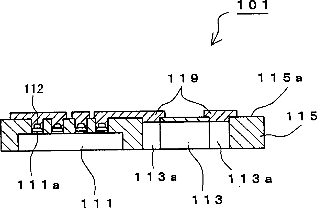
[0061] First, a manufacturing method for the electronic component mounted package 101 will be described. The process of mounting the semiconductor element 111 and the passive element 113 as electronic components into the substrate 115 includes a process of embedding the electronic components into the sheet-shaped substrate 115 from which electrodes 112 and 113a, and a process of forming a circuit pattern 119 electrically connected to the exposed electrodes 112 and 113. The description here exemplifies the case of forming a sheet module having the semiconductor element 111 and the passive element 113 embedded in a thermoplastic substrate as an example of the substrate 115 .

[0062] The thermoplastic base is preferably, for example, polyethylene terephthalate, polyvinyl chloride, polycarbonate, acrylonitrile butadiene styrene, thermoplastic polyimide or such material having electrically insulating properties, and The base thickness is 10μm-2.000mm. The thickness of the thermo...

no. 2 example

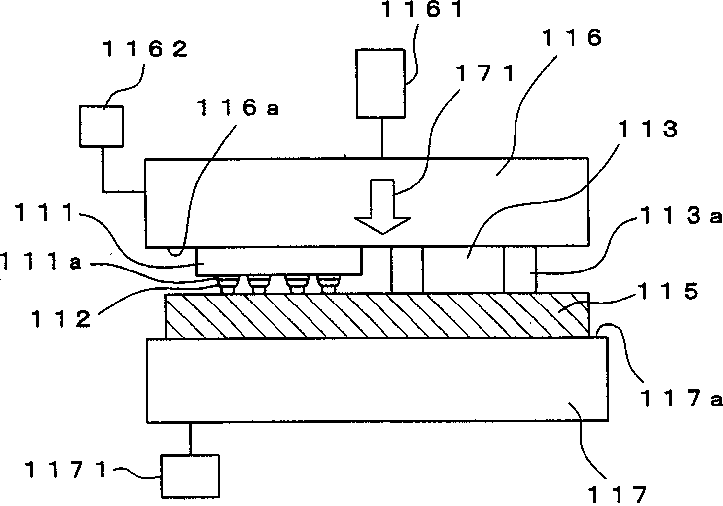
[0082] Figure 7 Shown is a sheet-shaped module corresponding to a component mounted with electronic components, which has a through hole 118 as a hole penetrating through a processed surface 115a of a thermoplastic sheet base 115 and a back surface 115d opposite to the processed surface 115a, and can be connected with figure 1 The illustrated assembly 101 mounted with electronic components compares the film capacitor 120 . The through hole 118 is formed by punching a hole in the thickness direction of the thermoplastic substrate 115 using a laser, a particle beam, or an electron beam. When the circuit pattern 119 is formed, a conductive material is provided to the inner outer surface of the through hole 118 or inside the through hole 118 at the same time. Thus, the electrical connection between the processed face 115a and the rear face 115d is achieved via the via hole 118 by at least one of conductive sputtering, vapor deposition, filling of a conductive material, and the ...

no. 3 example

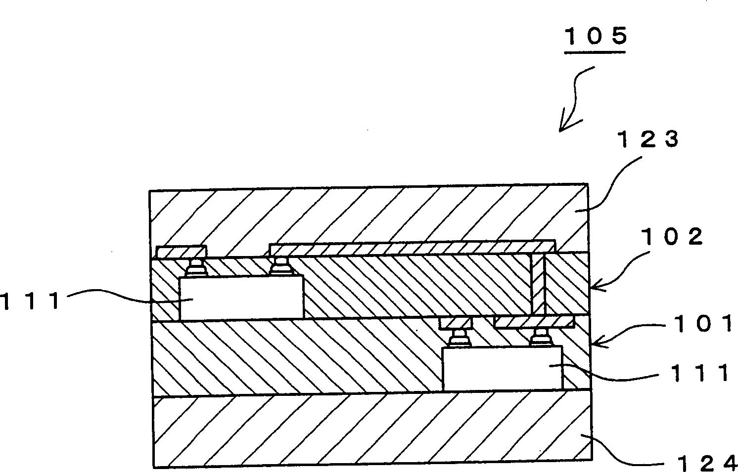
[0086] The electronic component mounted assembly 101 in the above first embodiment and the electronic component mounted assembly 102 in the above second embodiment are stacked in the thickness direction of the electronic component mounted assemblies 101 and 102, and by covering the The sheet-shaped protective materials 123 and 124 of the electronic component mounted components 101 and 102 are rolled to the electronic component mounted components 101 and 102, thereby manufacturing such as figure 2 A finished product 105 is shown with electronic components installed. The electronic component-mounted package 102 included in the electronic component-mounted finished product 105 of this third embodiment has no circuit pattern 119 formed on the back surface 115d. The electronic component-mounted assemblies 101 and 102 are aligned with each other such that the through hole 128 formed in the electronic component-mounted assembly 102 is electrically connected to the circuit pattern 11...


PUM

PropertyMeasurementUnit
thicknessaaaaaaaaaa
glass transition temperatureaaaaaaaaaa
heightaaaaaaaaaa

Abstract

A semiconductor element ( 111 ) with electrodes ( 112 ), and a passive element ( 113 ) with electrodes ( 113 a) are embedded in a thermoplastic sheet base ( 115 ), which is then subjected to laser beam machining, electron beam machining or ion beam machining to expose electrodes ( 112 and 113 a). Thereafter, a circuit pattern ( 119 ) is formed by formation of a thin film or printing of a conductive adhesive. Exposing the electrodes by laser beam machining or the like can be carried out in a short period of time and also by local treatment, thereby reducing damage to the base.

Description

technical field [0001] The present invention relates to a manufacturing method for electronic components-mounted components to manufacture electronic components-mounted components by mounting electronic components such as semiconductor components on a substrate, a A manufacturing method for an electronic component-mounted product having an electronic component mounted component, and an electronic component mounted product having an electronic component mounted component. The electronic-component-mounted finished product having the electronic-component-mounted assembly corresponds to a stack module, a memory card, a non-contact IC card, and the like. Background technique [0002] The following will refer to Figure 11 and Figure 12 A conventional manufacturing method for an electronic component-mounted finished product having, for example, a plurality of semiconductor components, capacitors, resistors, and such passive components mounted on a carrier substrate is described....

Claims


Application Information

Patent Timeline
Patent Type & Authority Applications(China)
IPC IPC(8): H05K1/16G06K19/077H01L21/56H01L21/60H01L23/12H01L23/498H01L23/538H01L25/00H05K1/18H05K3/46
CPCH01L2924/09701H01L2924/01039H01L2924/19105H01L2224/24195H01L24/24H01L2224/97H01L2924/01047H01L23/49855H01L2924/01046H01L2924/01004H01L2924/01072H01L2924/01006H01L2924/01078H01L2924/19041H01L23/5389H01L2924/01079H01L2924/01074H01L2924/01024H01L2224/73204H01L24/82H01L2924/01013H01L2924/014H01L2924/07811H05K1/185H01L2924/01029H01L24/97H01L2924/01018H01L2224/24226H01L2924/19043H01L2924/01019H01L2924/01033H01L21/568H01L2924/12042H01L2924/18162Y10T29/49155H01L2224/82H01L2924/00
Inventor 樱井大辅塚原法人
Owner PANASONIC CORP
Why Eureka
Try Eureka