Preparation of Y-Ba-Cu-O high temperature superconductive film

A high-temperature superconducting, yttrium barium copper oxide technology, which is applied in the usage of superconductor elements, the manufacture/processing of superconductor devices, superconducting devices, etc. Slow speed, increased preparation difficulty, etc., to achieve the effect of improving the weak connection of grain boundaries, low cost, and increasing critical current density

Inactive Publication Date: 2004-07-07
INST OF PHYSICS - CHINESE ACAD OF SCI
View PDF0 Cites 6 Cited by
  • Summary
  • Abstract
  • Description
  • Claims
  • Application Information

AI Technical Summary

Problems solved by technology

The composition and structure of the yttrium-barium-copper-oxygen superconducting layer grown by the PLD method are very good, but its growth rate is slow, the growth cost is expensive, and the difficulty of preparation increases rapidly as the film area becomes larger and thicker, as shown in the literature High critical current density YB 2 Cu 3 o 7-δ thick films using ion beam assisted deposition MgO bi-axially oriented template layers on nickel-based superalloy substrates, Journal of Materials Research--August 2001--Volume 16, Issue 8, pp.2175-2178. Introduced; using electron beam Co-evaporation method was used to prepare yttrium barium copper oxide film on RABiTS substrate, as described in the literature Electronbeam co-evaporation of Y-BaF2-Cu precursor films for YBa2Cu3O7-y coated conductors, supercond.Sci.Technol.14(April 2001) 218-223 Yes, but the electron gun and heat source used in this method need ultra-high vacuum, and the growth of high-temperature superconducting film requires oxygen, and the electron gun equipment must use high voltage, which makes the equipment of this method complicated and expensive. In addition, this method Generally, post-annealing treatment is required, and it is not suitable for the preparation of high-temperature superconducting thick films
In short, the above methods are not suitable for the preparation of high-temperature superconducting thick films, and cannot simply and quickly grow yttrium-barium-copper-oxygen superconducting tapes in batches.

Method used


Image

  • Preparation of Y-Ba-Cu-O high temperature superconductive film
  • Preparation of Y-Ba-Cu-O high temperature superconductive film
  • Preparation of Y-Ba-Cu-O high temperature superconductive film

Examples


Embodiment 1

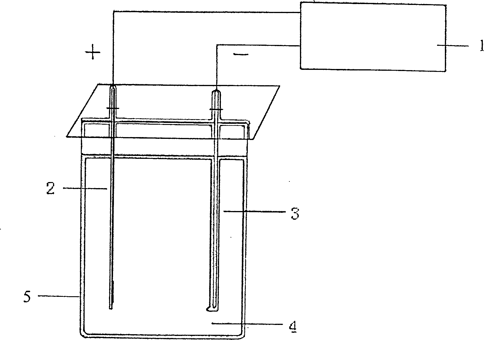
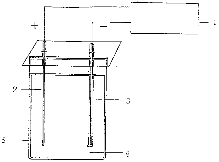
[0027] This embodiment is to prepare YBa on the MgO substrate of 5mm * 10mm 2 Cu 3 o 7-δ Nano superconducting film, using the battery 5, such as figure 1 As shown, the metal silver with a thickness of 0.3 mm, a width of 1.5 cm and a length of 5 cm is used as the positive and negative electrodes of the battery pool 5 after cleaning. The MgO substrate 6 of 10mm * 0.5mm is fixed on the negative electrode 3 after steaming a layer of Ag; Then, 2.45 grams of YBa 2 Cu 3 o 7-δ The powder is fully ground to make the particle size less than 2 μm, and then the ground YBa 2 Cu 3 o 7-δ The powder is prepared with a high-energy ball milling method to prepare nanoparticles with a particle size between 1-60nm, and mix it with 500 milliliters of acetone (purity 99.99%) with a glass rod and pour it into the electric pool 5; the negative electrode 3 with the baseband and the positive Electrode 2 is put into electric swimming pool, connects 900 volts of direct currents on electrode and ke...

Embodiment 2

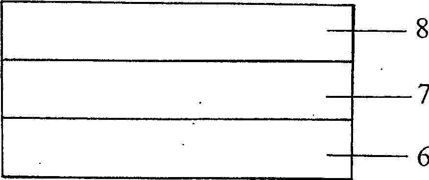
[0029] In this embodiment, YBa is prepared with chloroform as the electrophoretic solvent on the nickel sheet 6 with MgO as the isolation layer 10 mm × 40 mm in texture. 2 Cu 3 o 7-δ Nano-superconducting thin film. The electric pool 5 used, such as figure 1 As shown, first, a dense and uniform magnesium oxide film 7 is prepared on the nickel sheet 6, and then a layer of Pt is evaporated on the base tape and fixed on the negative electrode 3; YBa with a particle size of less than 0.5 μm 2 Cu 3 o 7-δ The powder is prepared by high-energy ball milling to prepare nanoparticles with a particle size in the range of 1-10nm, and mix with 1000 milliliters of chloroform (purity 99.99%), stir with a glass rod and pour into the electric pool; two electrodes are put into the electric pool 5, and the Connect the voltage of 900 volts between the positive and negative poles and keep it for 5 seconds. In this way, a layer of YBa with a thickness of about 100nm is deposited on the baseband...

Embodiment 3

[0031] In this embodiment, on a textured 20mm×80mm nickel sheet 6, MgO is used as an isolation layer 7 to grow YBa 2 Cu 3 o 7-δ Nano-superconducting thin film8. The electric pool 5 used, such as figure 1 As shown, first, a dense and uniform magnesium oxide film 7 is prepared on the nickel sheet 6, and then a layer of Al is evaporated on the MgO substrate; YBa with a particle size of less than 8 μm 2 Cu 3 o 7-δ The powder is prepared by high-energy ball milling method to prepare nanoparticles with a particle size between 1-60nm; fix the Al / MgO / Ni baseband on the negative electrode 3 and put it into the electric pool, and there is a voltage of 900 volts between the positive and negative electrodes, and keep 20 In this way, a layer of YBa with a thickness of about 300nm is deposited on the baseband 2 Cu 3 o 7-δ Nano superconducting film; finally, the deposited YBa 2 Cu 3 o 7-δ The nano-superconducting film is placed in a sintering furnace, and the temperature of the fu...


PUM

PropertyMeasurementUnit
particle sizeaaaaaaaaaa
thicknessaaaaaaaaaa
particle sizeaaaaaaaaaa

Abstract

This invention provides a semiconductor device that can prevent the leakage current increases when the TFT cuts off to improve the reliability and its manufacturing method, this semiconductor device has thin film transistor (TFT), the TFT has: semiconductor layer that contains channel region, source region and drain region; the grid insulated film set in the semiconductor layer; the grid electrode that controls conductivity of the channel region; there is a tiny convex on the surface of the semiconductor layer, the lateral inclining angle of the grid electrode is greater than inclining angle of the convex of the semiconductor layer.

Description

technical field [0001] The invention relates to the field of preparation of high-temperature superconducting films, in particular to a method for preparing high-temperature superconducting yttrium barium copper oxide (YBa 2 Cu 3 o 7-δ ) thick film method. Background technique [0002] Yttrium barium copper oxide (YBa 2 Cu 3 o 7-δ ) is one of the most valuable high-temperature superconductor materials with high irreversible lines, but YBCO has the disadvantage of weak connection, so it is difficult to prepare flexible superconducting strips by sheathing method, so people use a method called The method for growing the yttrium-barium-copper-oxygen superconducting film on the metal substrate of the second type of strip material; and directly growing the yttrium-barium-copper-oxygen superconducting film on the metal, the metal will diffuse into the conductor layer to deteriorate the superconductivity, resulting in Critical current density (J c )re...

Claims


Application Information

Patent Timeline
Patent Type & Authority Applications(China)
IPC IPC(8): C04B35/00C25D13/02H01B12/02H01L39/12H01L39/24
CPCY02E40/641Y02E40/60
Inventor 朱亚彬周岳亮王淑芳刘震陈正豪吕惠宾杨国桢
Owner INST OF PHYSICS - CHINESE ACAD OF SCI
Why Eureka
Try Eureka