Method for producing a bipolar transistor comprising a polysilicon emitter

A bipolar transistor, polysilicon technology, applied in transistors, semiconductor/solid-state device manufacturing, semiconductor devices, etc., can solve the problems of nitride barrier, inability to use the emitter window, filling and other problems

Inactive Publication Date: 2004-09-08
INFINEON TECH AG
View PDF0 Cites 3 Cited by
  • Summary
  • Abstract
  • Description
  • Claims
  • Application Information

AI Technical Summary

Problems solved by technology

However, the silicon layer formed in this way is usually relatively irregular, so this layer cannot be used to fill up the emitter window in practical applications.
[0009] As a further measure, the layer thickness of the polysilicon must be kept as low as possible, and the doping of the polysilicon must be kept as high as possible. Filling the emitter window with polysilicon should be avoided if possible, however, in higher In earlier technologies, this was made simpler by the larger size of the emitter, after depositing the polysilicon on the emitter, if a very narrow gap was left, depending on the technology chosen, when When etching the contact hole, additional effort is necessary because when other layers are deposited, the gap may be filled with unwanted species, i.e. nitride barrier

Method used


Image

  • Method for producing a bipolar transistor comprising a polysilicon emitter
  • Method for producing a bipolar transistor comprising a polysilicon emitter
  • Method for producing a bipolar transistor comprising a polysilicon emitter

Examples


Embodiment Construction

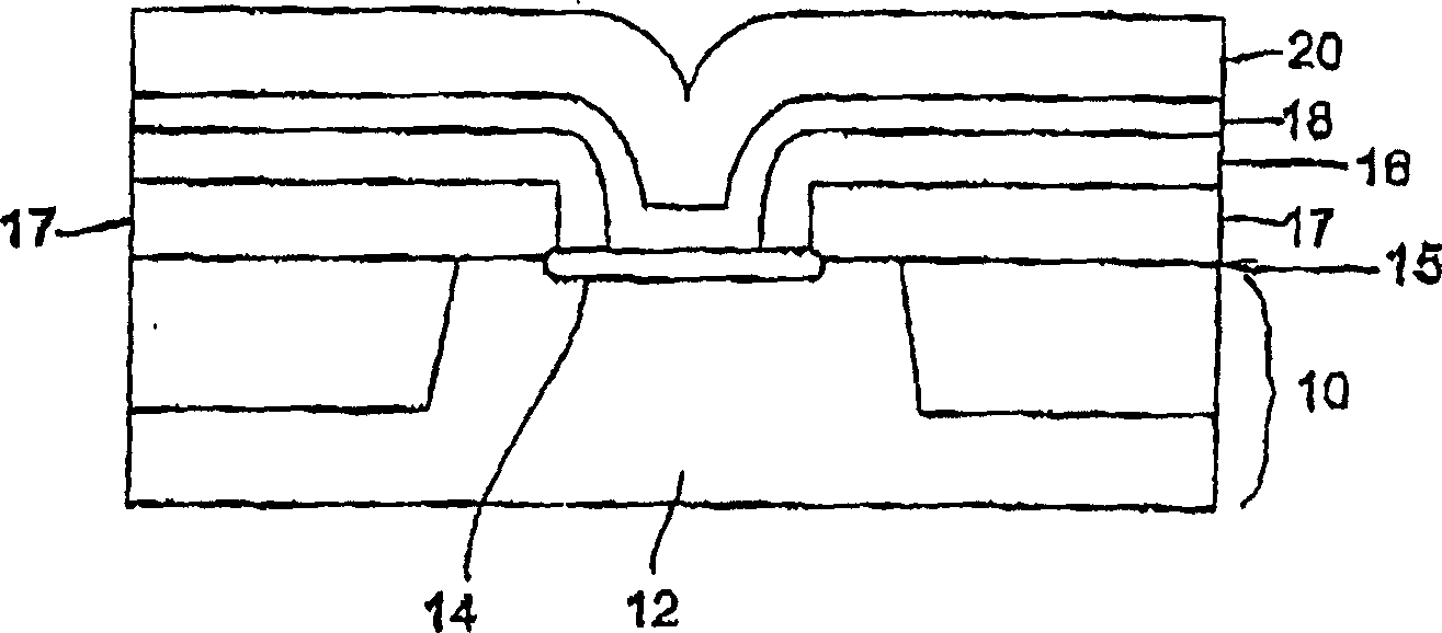
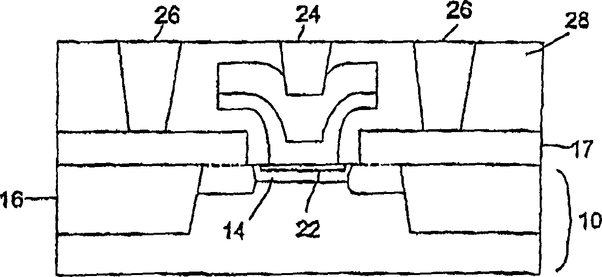
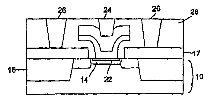
[0021] by figure 1 and figure 2 For reference, a preferred embodiment of the present invention for manufacturing bipolar transistors with polysilicon emitters will be explained in more detail.

[0022] Such as figure 1 As shown, preferably a monocrystalline silicon body is used as a substrate 10 for the bipolar transistor. In the substrate 10, a first region 12 of a first conductivity type is formed, which region 12 will later serve as a collector region. In the substrate 10 a further region 14 of a second conductivity type is formed, which then serves as a base region 14 .

[0023] In relation to the present case, the first conductivity type is denoted as so-called n-doped, while the second conductivity type is denoted as so-called p-doped, if the doping in the semiconductor material is in which the predominant charge carriers When the system is electrons, it is n-type, and the doping in the semiconductor material is p-type if the main charge carrier system is holes. In...


PUM


Abstract

In the inventive method for manufacturing a bipolar transistor having a polysilicon emitter, a collector region of a first conductivity type and, adjoining thereto, a basis region of a second conductivity type will be generated at first. At least one layer of an insulating material will now be applied, wherein the at least one layer is patterned such that at least one section of the basis region is exposed. Next, a layer of a polycrystalline semiconductor material of the first conductivity type, which is heavily doped with doping atoms, will be generated such that the exposed section is essentially covered. Now, a second layer of a highly conductive material on the layer of the polycrystalline semiconductor material will be generated in order to form an emitter double layer with the same. Thereupon, at least part of the doping atoms of the first conductivity type of the heavily doped polycrystalline semiconductor layer is caused to get into the basis region to generate an emitter region of the first conductivity type.

Description

technical field [0001] This case relates to inventions related to the manufacture of semiconductor devices, in particular to the manufacture of bipolar transistors with polysilicon emitters having reduced emitter resistance. Background technique [0002] Polysilicon emitters have been used in bipolar transistors designed to perform high power and high speed. The relationship between the theory and experiment of bipolar transistors with polysilicon emitters can be referred to Mr. C.R.Selvakumar published in IEEE Press No. 3 in 1988 - Article "Theoretical and Experimental Aspects of Polysilicon Emitter Bipolar Transistors" on page 16. [0003] Thus, an embodiment of a bipolar transistor with a polysilicon emitter provides a heavily doped polysilicon layer on the base, which acts as a plate (emitter / base )) a diffusion source for the transition state of the semiconductor, and may serve as a device in contact with the planar emitter. After performing the conventional processi...

Claims


Application Information

Patent Timeline
Patent Type & Authority Applications(China)
IPC IPC(8): H01L21/225H01L21/331
CPCH01L21/2257H01L29/66272H01L29/73
Inventor J·克里滋M·塞克A·蒂尔科
Owner INFINEON TECH AG
Why Eureka
Try Eureka