Method and apparatus for micro-jet enabled, low energy ion generation and transport in plasma processing

A plasma and plasma tube technology, which is used in the field of low-energy ion generation and transportation, and can solve problems such as temperature inconsistency and device damage.

Inactive Publication Date: 2004-12-08
LAM RES CORP
View PDF3 Cites 11 Cited by
  • Summary
  • Abstract
  • Description
  • Claims
  • Application Information

AI Technical Summary

Problems solved by technology

However, ion bombardment at such high energies can cause extensive damage to devices formed on the wafer
In addition, the extensive heating of wafers caused by bombardment by heavy ions may make individual wafers operate at inconsistent temperatures

Method used


Image

  • Method and apparatus for micro-jet enabled, low energy ion generation and transport in plasma processing
  • Method and apparatus for micro-jet enabled, low energy ion generation and transport in plasma processing
  • Method and apparatus for micro-jet enabled, low energy ion generation and transport in plasma processing

Examples


Embodiment Construction

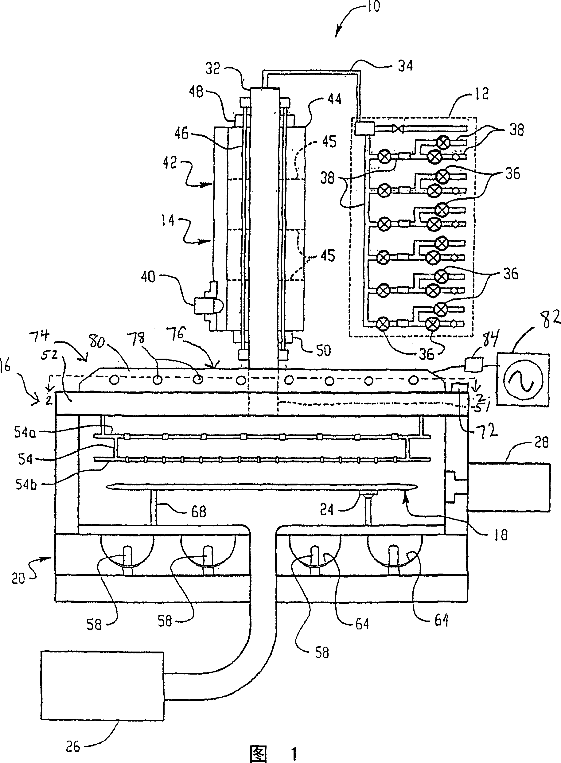
[0022] A novel low-energy ion generation and transport mechanism is presented here; this mechanism protects the wafer from high-energy ions caused by high sheath voltages while enhancing chemical decomposition and subsequent volatilization of the carbonized top layer of ion-implanted photoresist in a uniform manner. Potential harmful effects of ion bombardment. This soft ion-assisted technique has the advantage of achieving an optimal synergy between the ions produced by the auxiliary ion source within the incinerator and the chemicals already present, resulting in greater Faster response.

[0023] We believe that the ions contribute both the physical kinetic energy and the chemical internal energy released by the reaction, effectively lowering the activation energy of the surface reaction. By shielding the wafer from the high sheath potential characteristic of ordinary capacitive discharges, the ions experience a much weaker electric field as they pass through the sheath pot...


PUM


Abstract

A method for creating and transporting low-energy ions for use in plasma processing of a semiconductor wafer is disclosed. In an exemplary embodiment of the invention, the method includes generating plasma from a gas species to produce a plasma exhaust. The plasma exhaust is then introduced into a processing chamber containing the wafer. The ion content of the plasma exhaust is enhanced by activating a supplemental ion source as the plasma is introduced into the processing chamber, thereby creating a primary plasma discharge therein. Then, the primary plasma discharge is directed into a baffle plate assembly, thereby creating a secondary plasma discharge exiting the baffle plate assembly. The strength of an electric field exerted on ions contained in the secondary plasma discharge is reduced. In so doing, the reduced strength of the electric field causes the ions to bombard the wafer at an energy insufficient to cause damage to semiconductor devices formed on the wafer.

Description

[0001] Interaction with related applications [0002] This application is a partial continuation of the application with serial number 09 / 828.055 filed on April 6, 2001. technical field [0003] The present invention relates generally to plasma processing of semiconductor wafers, and more particularly to low energy ion generation and transport for use in plasma ashing systems. Background technique [0004] In integrated circuit manufacturing, photolithography is used to form integrated circuit patterns on substrates. Typically, a semiconductor substrate is coated with a photoresist material, a portion of which is exposed to ultraviolet (UV) radiation through a mask to image the desired circuit pattern on the photoresist. Those photoresists not exposed to UV radiation are then removed by a processing solution, leaving only the exposed portions on the substrate. In some cases, the remaining exposed portions are baked with UV light during the photostabilization process to ren...

Claims


Application Information

Patent Timeline
Patent Type & Authority Applications(China)
IPC IPC(8): H05H1/46H01J37/32H01L21/3065
CPCH01J37/32192H01J37/321H01L21/3065
Inventor A·斯里瓦斯塔瓦P·萨克蒂维尔H·萨温
Owner LAM RES CORP
Why Eureka
Try Eureka