Organic light-emitting device employing doped hole transporting layer and/or hole injecting layer

A technology for organic light-emitting devices and hole injection layers, which can be used in semiconductor/solid-state device manufacturing, household components, light-emitting materials, etc., and can solve problems such as impact and unfavorable luminous efficiency.

Active Publication Date: 2012-05-02
SAMSUNG DISPLAY CO LTD
View PDF2 Cites 0 Cited by
  • Summary
  • Abstract
  • Description
  • Claims
  • Application Information

AI Technical Summary

Problems solved by technology

However, this also promotes the outflow of charges from the emissive layer, which may adversely affect the luminous efficiency

Method used


Image

  • Organic light-emitting device employing doped hole transporting layer and/or hole injecting layer
  • Organic light-emitting device employing doped hole transporting layer and/or hole injecting layer

Examples


Embodiment 1

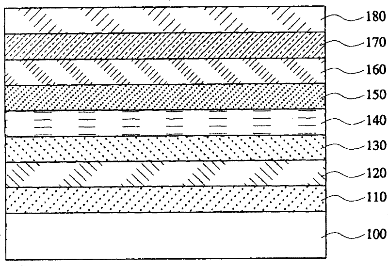
[0045] The anode is formed on the substrate using ITO (Indium Tin Oxide). On the substrate on which ITO has been formed: cleaning; 15 minutes UV-O 3 Treatment; coating with a mixed solution of BFE (obtained from Dow Chemical Company) and 5 wt % of 9,10-dicyanoanthracene (hereinafter referred to as "DCA") at an appropriate rotation speed and a thickness of 30 nm; and heat treatment. Thus, a hole injection layer was formed. The electron affinity of BFE is 2.46eV and that of DCA is 3.2eV.

[0046] On the substrate on which the hole injection layer has been formed, a hole transport layer, an emission layer, a hole blocking layer, an electron transport layer, an electron injection layer, and a cathode are sequentially formed, and sealed with a hygroscopic agent and a glass cover the substrate.

[0047] 30 nm of IDE320 (from IDEMITSU COMPANY) was used as the hole transport layer, and 20 nm of IDE140 (from IDEMITSU COMPANY) containing 6 wt% of IDE105 was used as the emission laye...

Embodiment 2

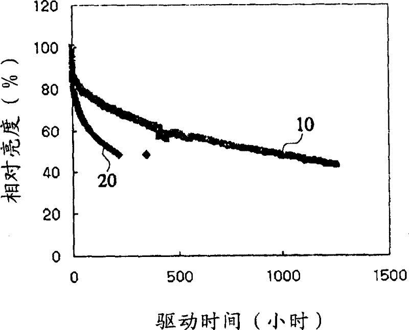
[0049] An organic light-emitting device was prepared in the same manner as in Example 1, except that a hole transport layer was not formed.

Embodiment 3

[0061] Prepare an organic light-emitting device in the same manner as in Example 1, except that the mixed solution of BFE and 5wt% DCA is coated with a thickness of 25nm on the substrate on which ITO has been formed to form a hole injection layer, and then A hole transport layer with a thickness of 25 nm was formed on the hole injection layer using IDE320.


PUM


Abstract

An organic light-emitting device including an anode, a cathode, an emission layer interposed between the anode and the cathode, and at least one of the hole injecting layer and the hole transporting layer interposed between the anode and the emission layer, wherein the at least one of the hole injecting layer and the hole transporting layer includes a host material, and a dopant material as an electron acceptor, wherein the dopant material has an electron affinity greater than that of the host material by at least 0.1 eV.

Description

[0001] Cross References to Related Applications [0002] This application claims priority from Korean Patent Application No. 2003-41250 filed with the Korean Intellectual Property Office on June 24, 2003, the disclosure of which is incorporated herein by reference. technical field [0003] The present invention relates to an organic light emitting device (OLED), more particularly, the present invention relates to an organic light emitting device having a doped hole transport layer (HTL) and / or hole injection layer (HIL). Background technique [0004] Organic light-emitting devices such as self-emitting displays have ideal structures: compact, light in weight, simple in composition and process. OLEDs also have several other advantages, such as the ability to ensure high resolution and wide viewing angle, the ability to achieve excellent moving images and high contrast, and electrical characteristics suitable for mobile devices because low power consumption and low voltage ar...

Claims


Application Information

Patent Timeline
Patent Type & Authority Patents(China)
IPC IPC(8): H01L51/52C09K11/06H05B33/26H01L51/50H05B33/12H05B33/20
CPCH01L51/5088H01L51/5052Y10S428/917H10K50/155H10K50/17H05B33/26
Inventor 徐旼撤杨南喆陈炳斗金茂显李城宅
Owner SAMSUNG DISPLAY CO LTD
Why Eureka
Try Eureka