

Organic electro-white light device and producing method thereof
A white light device and electroluminescent technology, applied in the direction of electroluminescent light source, chemical instrument and method, electric light source, etc., can solve the problem of low efficiency and achieve the effect of improving utilization rate
- Summary
- Abstract
- Description
- Claims
- Application Information
AI Technical Summary
Problems solved by technology
Method used
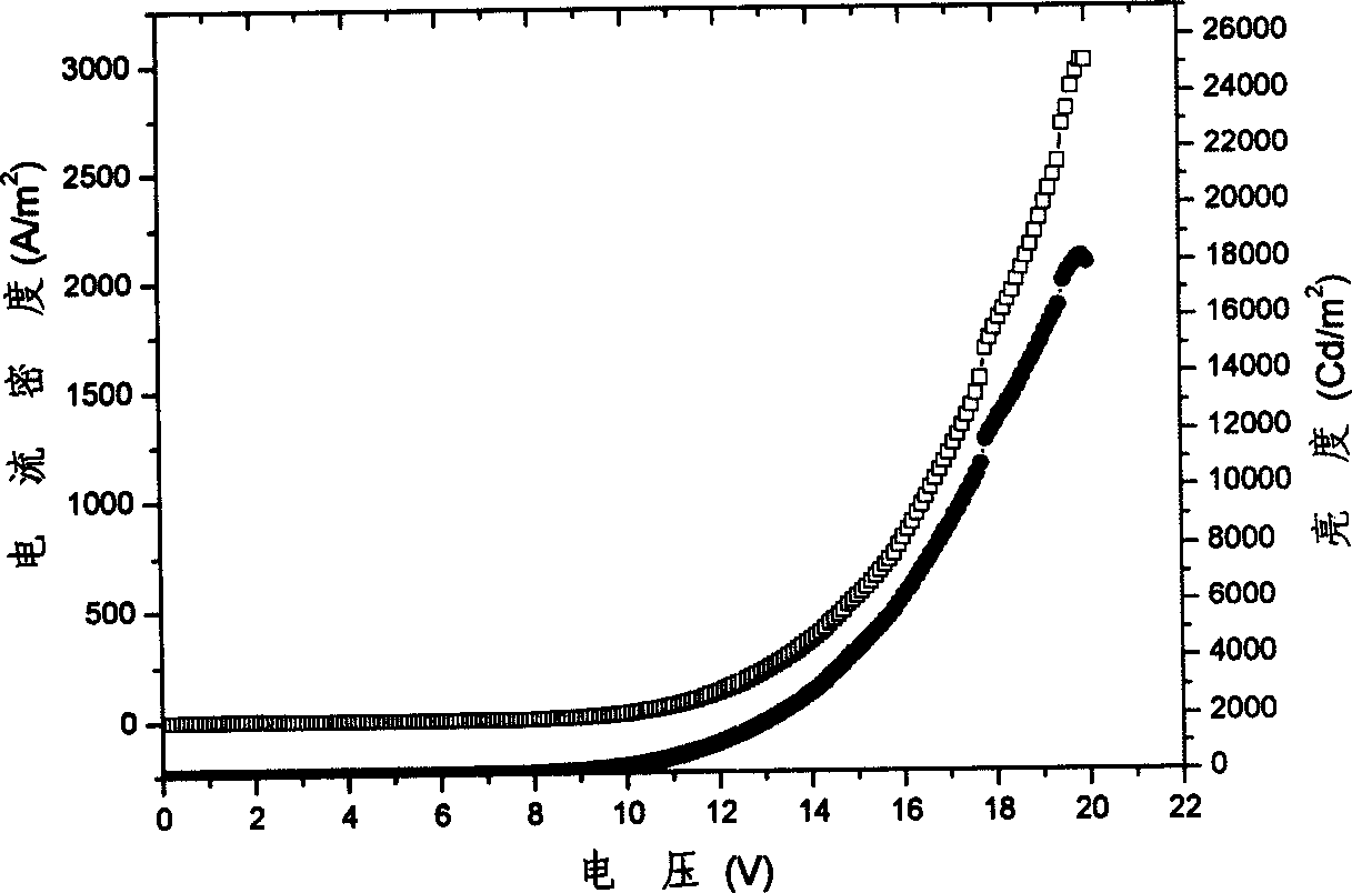
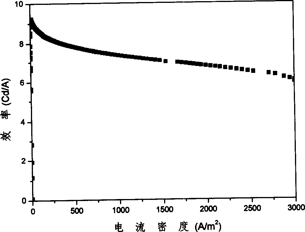
Image

Examples
Embodiment 1
[0070] Embodiment 1 (device number OLED1)
[0071] OLED1 was prepared by the method for preparing the device represented by structural formula (1).
[0072] The hole transport layer in OLED1 is NPB, the host material in the organic light-emitting layer is DCB, the phosphorescent dye is FIrpic and the red dye is DCJTB, the electron transport layer is Bphen, and the cathode layer is Mg:Ag alloy and Ag.
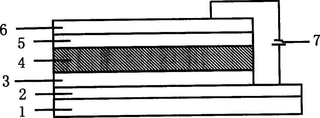
[0073] Glass / ITO / NPB / DCB:FIrpic:DCJTB / Bphen / Mg:Ag / Ag
[0074] The preparation method is as follows:
[0075] ① Clean the transparent conductive substrate ITO glass by using hot detergent ultrasonic and deionized water ultrasonic method. Pretreatment of ion beam bombardment, in which the ITO film on the conductive substrate is used as the anode layer of the device, the square resistance of the ITO film is 15Ω, and the film thickness is 200nm;
[0076] ② Put the above-mentioned cleaned, dried and pretreated ITO glass in a vacuum chamber, and evacuate to 1×10 -5 ~9×10 -3 Pa, a...
Embodiment 2
[0081] Embodiment 2 (device number OLED2)
[0082] OLED2 was prepared by the method for preparing the device represented by structural formula (1).
[0083] The host material in the organic light-emitting layer in OLED2 is CBP, the phosphorescent dye is FIr6 and the red dye is DCM, the electron transport layer is BAlq, and the cathode layer is alternate layers of LiF and Al.
[0084] Glass / IT0 / CBP:Fir6:DCM / BAlq / LiF / Al
[0085] The method for preparing the light-emitting layer and the electron transport layer in OLED2 is the same as in Example 1, wherein the film thickness of the light-emitting layer is 30nm, the doping concentration of FIr6 is 3wt%, the doping concentration of DCM is 0.05wt%, and the film thickness of BAlq is 40nm.
[0086] The method for preparing the cathode layer is as follows: keep the pressure in the above-mentioned vacuum chamber constant, and sequentially vapor-deposit a LiF layer and an Al layer on the above-mentioned BAlq electron transport layer as ...
Embodiment 3
[0088] Embodiment 3 (device number OLED3)
[0089] OLED3 was prepared by the method for preparing the device represented by structural formula (2).
[0090] Glass / ITO / PEDOT / PVK:PBD:FIrpic:Rubrene / Bphen / Mg:Ag / Ag
[0091] The preparation method is as follows:
[0092] ① Clean the transparent conductive substrate ITO glass by using hot detergent ultrasonic and deionized water ultrasonic method. Pretreatment of ion beam bombardment, in which the ITO film on the conductive substrate is used as the anode layer of the device, the square resistance of the ITO film is 30Ω, and the film thickness is 200nm;
[0093] ②Spin-coat a layer of 60nm-thick PEDOT as the anode buffer layer, and dry it with an infrared lamp. PVK was used as the matrix and hole transport material, PBD was used as the electron transport material, and PVK and PBD were dissolved in chloroform at a ratio of 9:1. Both FIrpic and Rubrene were dissolved in chloroform separately. Draw corresponding volumes of the three...
PUM
| Property | Measurement | Unit |
|---|---|---|
| thickness | aaaaa | aaaaa |
| thickness | aaaaa | aaaaa |
Abstract
Description
Claims
Application Information