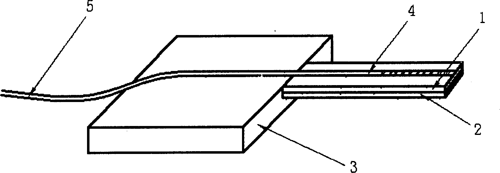
Bragg raster hydrogen sensor and its preparing process
A preparation process and sensor technology, applied in the Bragg grating hydrogen sensor and its preparation field, can solve the problems of increased film thickness, easy damage and the like
- Summary
- Abstract
- Description
- Claims
- Application Information
AI Technical Summary
Problems solved by technology
Method used
Image
Examples
Embodiment 1
[0023] 1. Use sputtering method to make Cr / Cu primer on single crystal silicon substrate thick;
[0024] 2. Electroplate a 20μm thick Cu film as the support seat of the micro-cantilever beam. The length and width of the support are 4×4mm;
[0025] 3. A metal Pd film with a thickness of 200nm is deposited on the Cu film by magnetron sputtering as a sensitive film for absorbing hydrogen;
[0026] 4. Next, spin-coat a 10 μm thick AZ4620 photoresist on the metal Pd film, photolithography, develop and electroform a 10 μm thick nickel film as a part of the drive beam;
[0027] 5. Remove photoresist;
[0028] 6. Using the Ni film as a mask, etch away the metal Pd with a thickness of 200nm by dry method;
[0029] 7. Wet etch the Cu film under the Pd film as the sacrificial layer. Since the length and width of the beam are 8mm and 2mm respectively, when the Pd film is leaked, a part of Cu remains at the support as the support of the cantilever beam.
[0030] 8. Select the Bragg wa...
Embodiment 2
[0034] 1. Use sputtering method to make Cr / Cu primer on single crystal silicon substrate thick;
[0035] 2. Electroplate a 30μm thick Cu film as the support seat of the micro-cantilever beam. The length and width of the support are 4×4mm;
[0036] 3. A metal Pd film with a thickness of 300nm is deposited on the Cu film by magnetron sputtering as a sensitive film for absorbing hydrogen;
[0037] 4. Next, spin-coat 20 μm thick AZ4620 photoresist on the metal Pd film, photolithography, develop and electroform a 10 μm thick nickel film as part of the drive beam;
[0038] 5. Remove photoresist;
[0039] 6. With a Ni film micro-mask, etch away the metal Pd with a thickness of 300nm by dry method;
[0040] 7. Wet etch the Cu film under the Pd film as the sacrificial layer. Since the length and width of the beam are 8mm and 2mm respectively, when the Pd film is leaked, a part of Cu remains at the support as the support of the cantilever beam.
[0041] 8. Select the Bragg waveleng...
Embodiment 3
[0045] 1. Use sputtering method to make Cr / Cu primer on single crystal silicon substrate thick;
[0046] 2. Electroplate a 40μm thick Cu film as the support seat of the micro-cantilever beam. The length and width of the support are 4×4mm;
[0047] 3. A metal Pd film with a thickness of 500nm is deposited on the Cu film by magnetron sputtering as a sensitive film for absorbing hydrogen;
[0048]4. Next, spin-coat 20 μm thick AZ4620 photoresist on the metal Pd film, photolithography, develop and electroform a 10 μm thick nickel film as part of the drive beam;
[0049] 5. Remove photoresist;
[0050] 6. Using a Ni film micro-mask, etch away the metal Pd with a thickness of 500nm by dry method;
[0051] 7. Wet etch the Cu film under the Pd film as the sacrificial layer. Since the length and width of the beam are 8mm and 2mm respectively, when the Pd film is leaked, a part of Cu remains at the support as the support of the cantilever beam.
[0052] 8. Select the Bragg waveleng...
PUM
 Abstract
Description
Claims
Application Information
