Electrical component assembly and method of fabrication

A technology for electrical components and components, applied in the direction of electrical components, assembling printed circuits with electrical components, and manufacturing printed circuits, etc. problems, resulting in shorter manufacturing cycle times, improved electrical performance, and improved reliability

Inactive Publication Date: 2005-05-25
NANOPIERCE TECH
View PDF2 Cites 12 Cited by
  • Summary
  • Abstract
  • Description
  • Claims
  • Application Information

AI Technical Summary

Problems solved by technology

[0011] 2. The reflow of the solder joints and then filling and hardening the encapsulant results in reduced productivity; and
[0012] 3. The flux residue left in the gap between the chip and the substrate reduces the adhesive strength and cohesive strength of the sealing adhesive of the filler, thereby affecting the reliability of the component
However, this technique is difficult to use in fabricating connections required to selectively interconnect electrical components such as integrated circuits with multiple contact pads to printed circuit boards

Method used


Image

  • Electrical component assembly and method of fabrication
  • Electrical component assembly and method of fabrication
  • Electrical component assembly and method of fabrication

Examples


example 1

[0094] The following process is used to prepare the metallized contacts on the copper flex circuit, more specifically the metallized contacts to be used to electrically connect the flex circuit to the antenna coil within the body of the smart card.

[0095] To form the base nickel metallization, test samples were taken with patterned copper traces and contact pads overlying the flexible circuit substrate. The test samples also included a layer of photoresist covering the copper traces and exposing the contact pads. For the purpose of the experiment, the flexible circuit test substrate was obtained from Multitape GmbH, Salzkotten, Germany.

[0096] Metallization of the contact pads was produced by electroplating nickel on the base copper pad in a first nickel plating bath to a height of about 70 microns. The bath contained nickel sulfamate ("Electropure 24" from Atotech (State College), Pennsylvania, USA) at 80 g / L nickel and nickel bromide in a nickel electroplating solution ...

example 2

[0100] The test samples described in Example 1 were plated in the first nickel plating bath for about 2 minutes. A second plating bath was prepared when using the nickel plating solution described in Example 1, but instead of nickel plated diamond particles, commercial grade silicon carbide particles from Fujimi Industries were increased to a concentration of about 1 gram / liter. The silicon carbide particles are about 14 microns in size. Electroplating process at about 100A / ft 2 is performed at current densities. Also, the agitation in the tank is turned off immediately before the sample is submerged in the tank. After electroplating the silicon carbide layer, the sample was returned to the first electroplating tank for 6 minutes to form an adherent layer covering the particle layer.

example 3

[0102] The test samples described in Example 1 were plated in the first nickel plating bath for about 12 minutes. A second plating bath was prepared using the plating solution described in Example 1, but instead of the nickel-plated diamond particles, uncoated, 14 micron diamond particles were added to the bath to a concentration of 1 g / L. The agitation in the tank was turned off, and the test sample was submerged in the tank for a period of time sufficient to form a diamond layer of about 25 to 35 microns in thickness. Electroplating process at about 100A / ft 2 is performed at current densities. After electroplating in the particle tank, the samples were returned to the first plating tank for 7 minutes to form an adherent layer covering the diamond particle layer.


PUM

PropertyMeasurementUnit
modulusaaaaaaaaaa
modulusaaaaaaaaaa
thicknessaaaaaaaaaa

Abstract

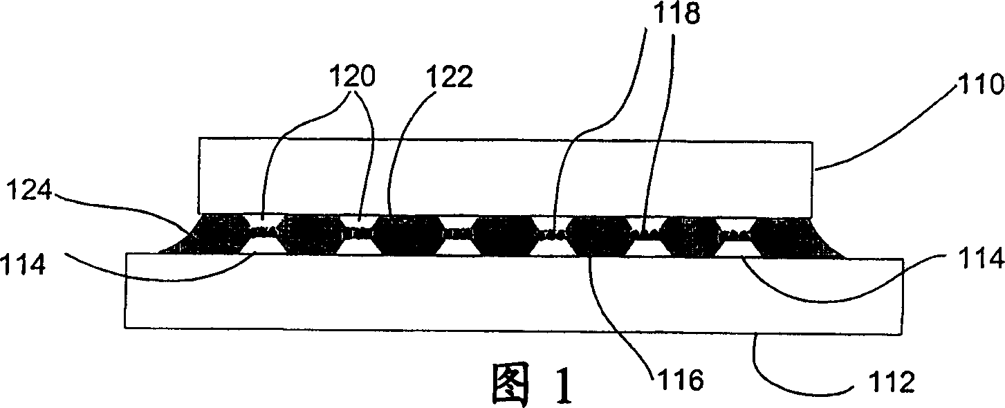
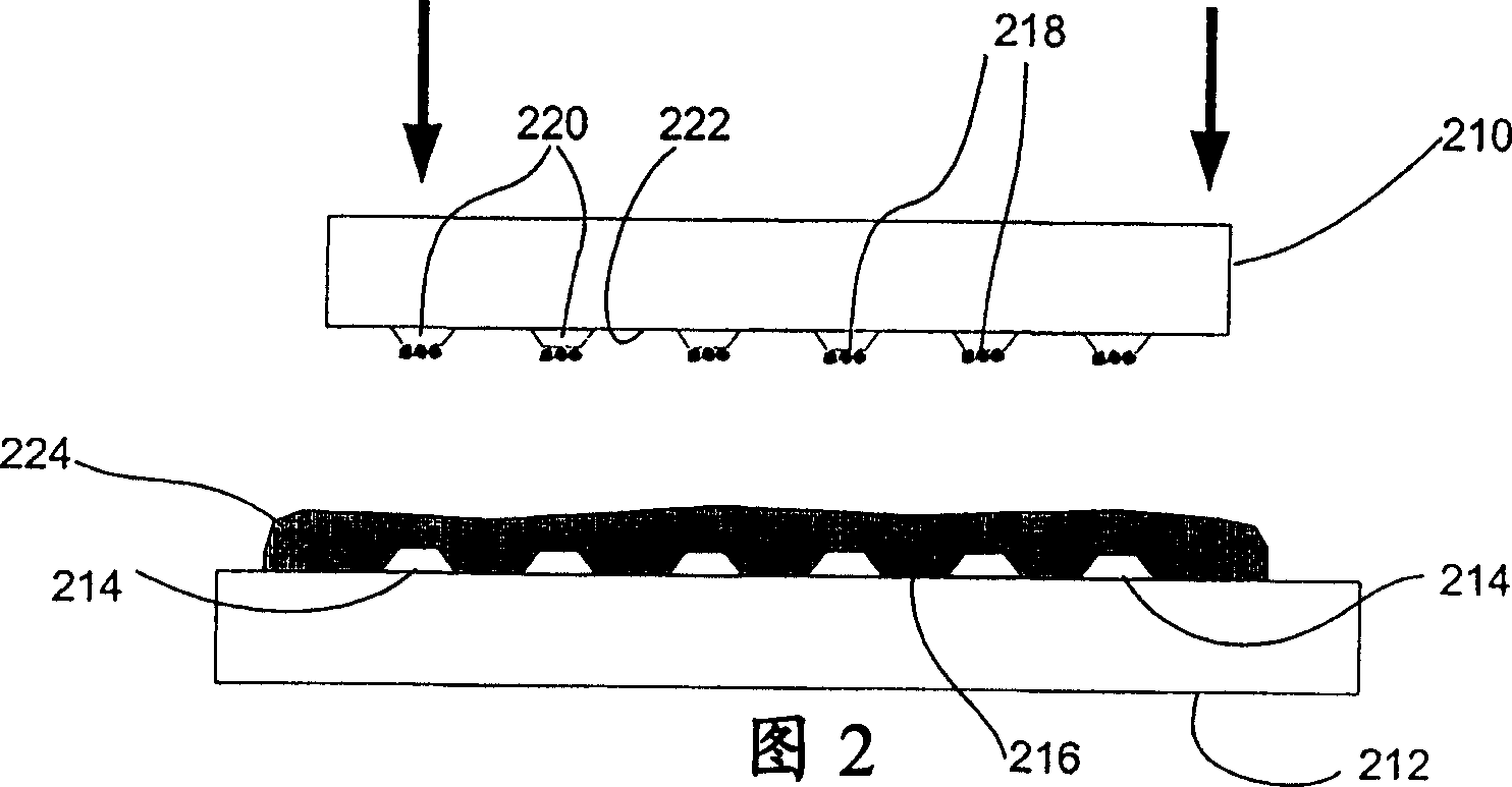
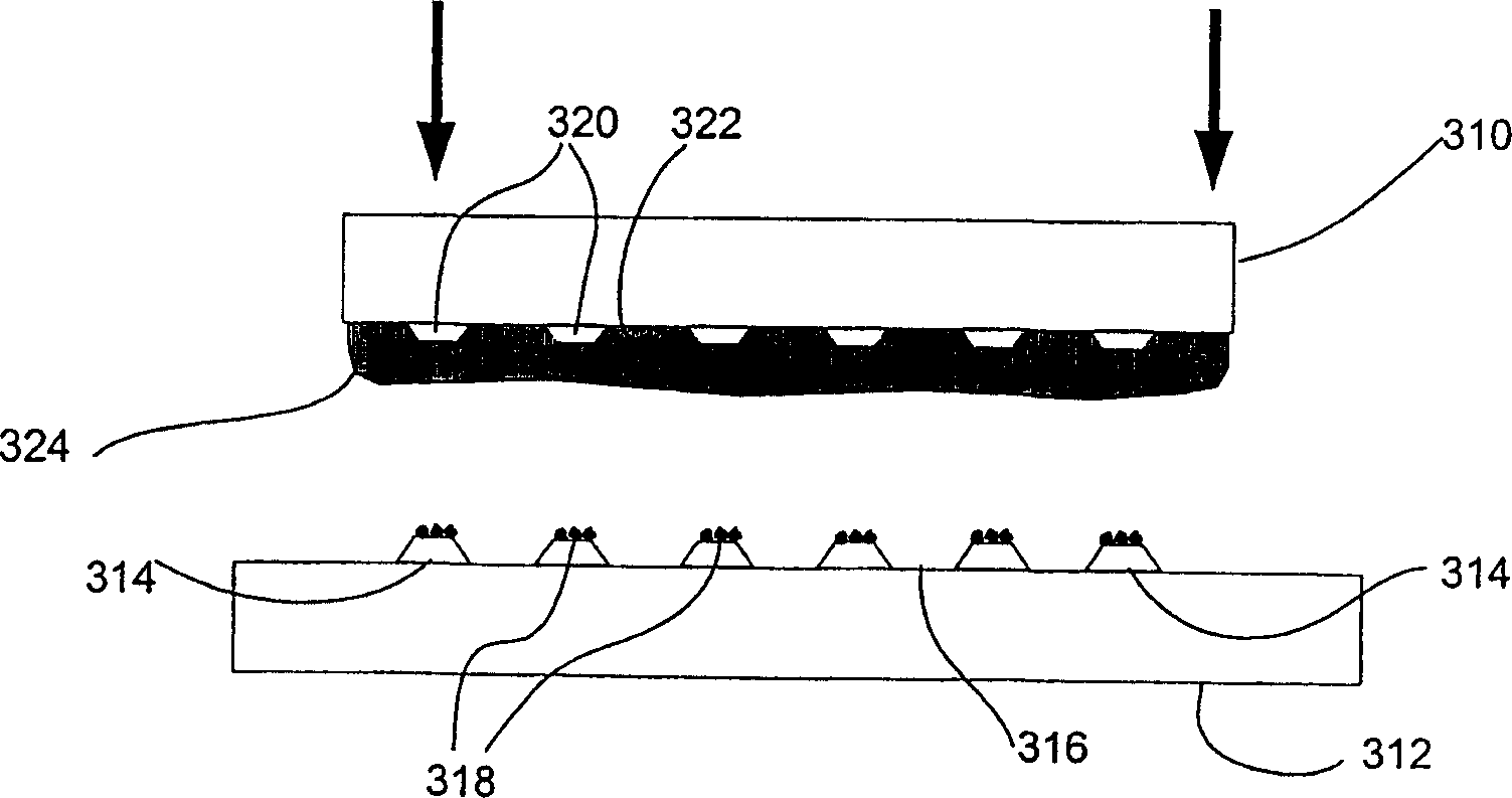
An electrical component assembly and method of manufacturing the same, wherein particles (318) are fixed to a metal surface (314) and pressure is applied to cause the particles to penetrate at least one metal contact surface (314). In one method, hard particles (318) are applied to one of the metal surfaces (314) by electroplating the particles in an electroplating bath. In another approach, hard particles (318) are applied to a non-conductive adhesive layer (324) positioned between the electronic component (310) and the substrate (312). Once pressure is applied to the electronic component (310) or substrate (312), a permanent, conductive bond is formed.

Description

[0001] REFERENCE TO RELATED APPLICATIONS [0002] This application is related to and claims the benefit of priority from the following application, which is hereby incorporated by reference: US Application Serial No. 09 / 684,238, filed October 5, 2000, entitled "Assemblies and Methods of Making Electrical Components," ( "Electrical Component Assembly and Method of Fabrication,"), US Provisional Application Serial No. 60 / 220,027, filed July 21, 2000, entitled "Advances in Materials for Low-Cost Flip Chips" ("Advances in Materials for Low Cost Flip-Chip,"), US Provisional Application Serial No. 60 / 233,561, filed September 19, 2000, entitled "Manufacturing of Low Cost SmartLabels," . technical field [0003] The present invention relates generally to electrical component assemblies and methods of manufacturing the same, and more particularly to structures and methods for electrical and mechanical connections of semiconductor flip-chips and flip-chip micro-assemblies to substrates...

Claims


Application Information

Patent Timeline
Patent Type & Authority Applications(China)
IPC IPC(8): G06K19/077H01L21/56H01L21/60H01L23/485H01L23/498H05K3/28H05K3/32H05K3/36H05K3/40
CPCG06K19/07752G06K19/07769H01L21/563H01L23/49811H01L24/31H01L24/83H01L2224/13099H01L2224/16225H01L2224/73203H01L2224/7565H01L2224/83101H01L2224/83191H01L2224/83192H01L2924/01004H01L2924/01005H01L2924/01011H01L2924/01012H01L2924/01013H01L2924/01015H01L2924/0102H01L2924/01022H01L2924/01027H01L2924/01029H01L2924/01032H01L2924/01033H01L2924/01038H01L2924/01046H01L2924/01047H01L2924/01049H01L2924/0105H01L2924/01051H01L2924/01056H01L2924/01078H01L2924/01079H01L2924/01082H01L2924/01327H01L2924/0781H01L2924/14H01L2924/19041H01L2924/19043H05K3/325H05K3/4007H01L2224/2919H01L2924/01006H01L2924/01019H01L2924/01023H01L2924/01037H01L2924/01055H01L2924/014H01L2924/0665H01L24/29H01L2224/73204H01L2224/73104H01L2224/32225H01L2924/10253H01L24/13H01L2924/07802H01L2224/29499H01L2224/2929H01L2224/293H01L2224/81193H01L2224/83851H01L2224/13H01L2924/00014H01L24/16H01L2924/00H01L2924/3512H01L2224/0401H01L21/60H01L24/10
Inventor 赫伯特·J·诺伊豪斯迈克尔·J·肯尼迈克尔·E·沃纳
Owner NANOPIERCE TECH
Why Eureka
Try Eureka