
Low contact resistance low light absorption and full angle high reflectance LED electrode

A technology of low contact resistance and light absorption, applied in circuits, electrical components, semiconductor devices, etc., can solve the problems of low contact resistance and low light absorption characteristics of electrodes

Inactive Publication Date: 2005-06-01
BEIJING TIMESLED TECH CO LTD
View PDF0 Cites 9 Cited by
  • Summary
  • Abstract
  • Description
  • Claims
  • Application Information

AI Technical Summary

Problems solved by technology

[0003] The technical problem to be solved by the present invention is that the existing electrodes cannot have low contact resistance and low light absorption characteristics at the same time. To obtain low contact resistance like metal electrodes and reduce light absorption as much as possible to improve thermal reliability, that is, P-GaN high The main problem that the counter electrode needs to solve

Method used


Image

  • Low contact resistance low light absorption and full angle high reflectance LED electrode
  • Low contact resistance low light absorption and full angle high reflectance LED electrode
  • Low contact resistance low light absorption and full angle high reflectance LED electrode

Examples


Embodiment approach 1

[0021] like Figure 4 As shown, the electrode is composed of protective layer Au film 4, Ag high reflection mirror 3, porous ohmic contact layer 8, low refractive index SiO 2 The transparent film 9, the doped semiconductor 1, etc. are composed, and the specific manufacturing steps are as follows:

[0022] 1) A 300 μm × 300 μm LED sample was prepared on a sapphire by a common metal-organic chemical vapor deposition (MOCVD) method. 17 cm -3 .

[0023] 2) The sample is cleaned by common chemical cleaning method: HCl: H 2 The surface of the GaN in the P region was cleaned with a solution of 1:1 O for 5 minutes, and then washed with deionized water for 5 times. After washing with dry N 2 Air dry.

[0024] 3) Put the sample into the reaction chamber of Denton Discovery550 evaporation platform quickly, and pump the reaction chamber to 10 -5 Background vacuum below Pa.

[0025] 4) Plating 2.5nm Ni and 6nm Au at a rate of 2 Å / s at 70°C, using a Karl Suss lithography machine, co...

Embodiment approach 2

[0033] Such as Figure 4 As shown, the electrode is composed of protective layer Au film 4, Ag high reflection mirror 3, porous ohmic contact layer 8, low refractive index indium tin oxide film 9, doped semiconductor 1, etc. The specific manufacturing steps are as follows:

[0034] 1) A 300 μm × 300 μm LED sample was prepared on a sapphire by a common metal-organic chemical vapor deposition (MOCVD) method. 17 cm -3 .

[0035] 2) The sample is cleaned by common chemical cleaning method: HCl: H 2 The surface of the GaN in the P region was cleaned with a solution of 1:1 O for 5 minutes, and then washed with deionized water for 5 times. After washing with dry N 2 Air dry.

[0036] 3) Put the sample into the reaction chamber of Denton Discovery550 evaporation platform quickly, and pump the reaction chamber to 10 -5 Vacuum below Pa.

[0037] 4) Plating 4nm Ni at a rate of 3 Å / s at 70°C.

[0038] 5) Using a Karl Suss photolithography machine, a common photolithography process...

Embodiment approach 3

[0047] 1) A 300 μm × 300 μm LED sample was prepared by the common metal-organic chemical vapor deposition (MOCVD) method, the P-GaN substrate thickness was 1.5 μm, and the Mg doping was 5 × 10 17 cm -3 .

[0048] 2) The sample is cleaned by common chemical cleaning method: HCl: H 2 The surface of the GaN in the P region was cleaned with a solution of 1:1 O for 5 minutes, and then washed with deionized water for 5 times. After cleaning for N 2 Air dry.

[0049] 3) Put the sample into the reaction chamber of Denton Discovery550 evaporation platform quickly, and pump the reaction chamber to 10 -5 Vacuum below Pa.

[0050] 4) Plating 2nm Ni and 2nm Pt at a rate of 3 Å / s at 70°C.

[0051] 5) Using a Karl Suss photolithography machine, a common photolithography process and an etching process are used to make microholes with a radius of 3 μm on the Ni / Pt layer. Microholes communicate with P-GaN. The distance between the centers of adjacent microwells is 22 μm. 20 μm is left ...


PUM

PropertyMeasurementUnit
Total thicknessaaaaaaaaaa
Radiusaaaaaaaaaa
Contact resistivityaaaaaaaaaa

Abstract

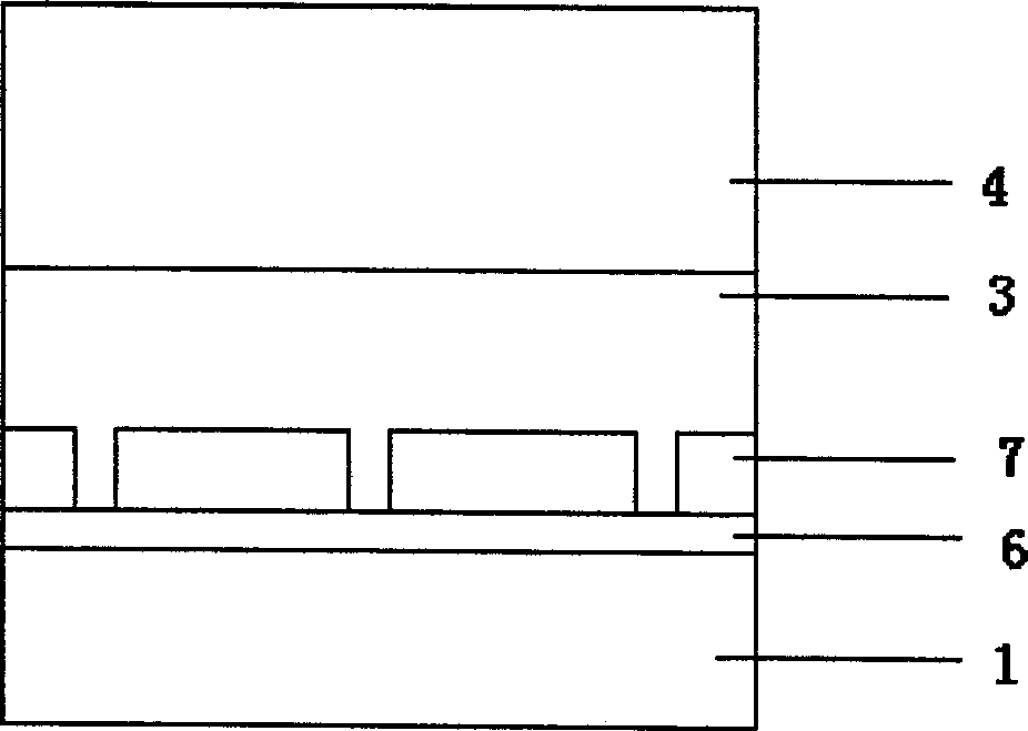
The present invention relates to one kind of LED electrode with low contact resistance, low light absorption and high reflectivity, and belongs to the field of the photoelectronic device making technology. The electrode has the structure including the first layer of semiconductor substrate, the second layer of ohmic contact layer on the semiconductor substrate, the third layer of high reflectivity Ag mirror on the ohmic contact layer and the fourth layer of protecting layer on the high reflectivity Ag mirror. The present invention features that the ohmic contact layer has circular through micropores with coated transparent film with the optimal optical thickness in one quarter of wavelength of light the device emits and the refractive index smaller than the complex refractive index of the semiconductor substrate and the high reflectivity Ag mirror so as to form structure of high-low-high refractive index. The electrode has low contact resistance, less light absorption and high heat reliability.

Description

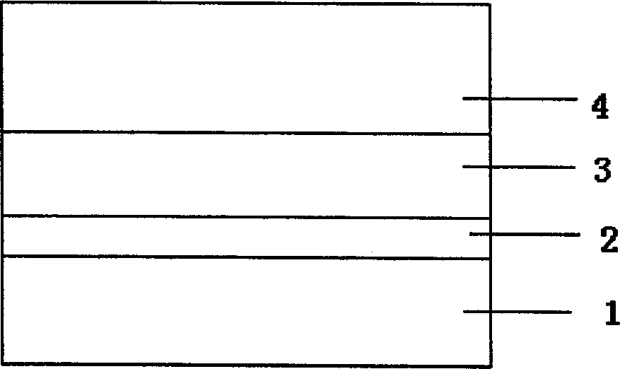
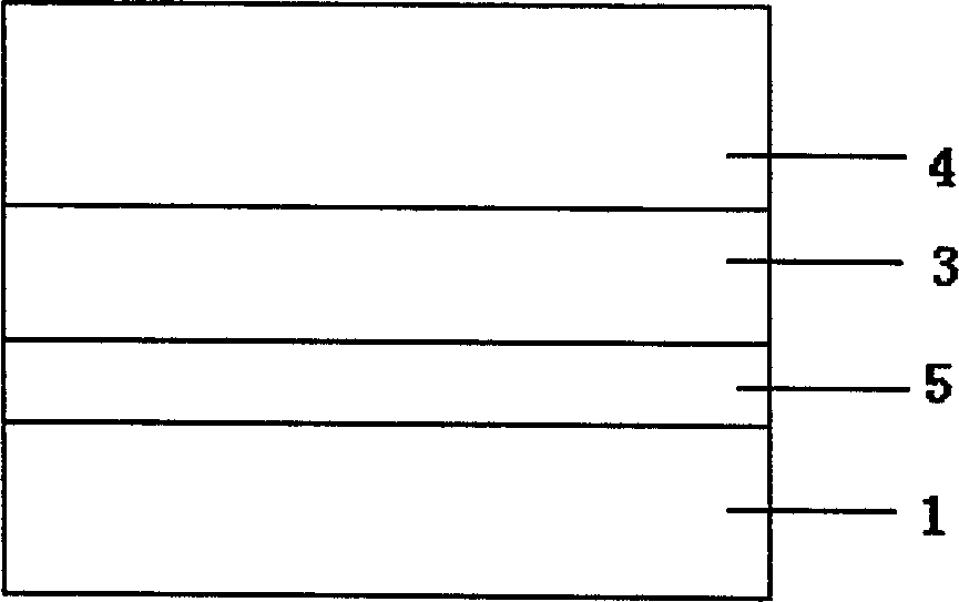
technical field [0001] The invention is used in the technical field of optoelectronic device manufacturing, and in particular relates to a light emitting diode (LED) electrode structure. Background technique [0002] The traditional high-reverse electrode Ni / Au / Ag (see figure 1 ), transparent conductive oxide film (TCO) coated silver high reflective mirror (see figure 2 ) and other flat electrodes. The Ni / Au / Ag electrode is composed of a doped semiconductor layer 1, a Ni / Au ohmic contact layer 2, a silver high reflection mirror 3 and a protective film 4. This electrode has a low specific contact resistance, and its specific contact resistivity can be as low as 10 -6 Ω·cm 2 . But the disadvantage is that the metal contact layer absorbs light seriously, and the light absorption coefficient K is greater than 1, and increases with the increase of its thickness and area. It causes a serious loss of light output power, the absorption of 460nm blue light reaches 20%-30%, and...

Claims


Application Information

Patent Timeline
IPC IPC(8): H01L33/00
Inventor 沈光地朱彦旭李秉臣郭霞董立闽
Owner BEIJING TIMESLED TECH CO LTD
Learn More