Method for online test of wafer metal interconnection line reliability

A technology of metal interconnection and online testing, applied in semiconductor/solid-state device testing/measurement, electrical components, electrical solid-state devices, etc., can solve the problem of complex detection process, affecting IC process yield, and inability to detect insulating dielectric materials on-line Layer reliability and other issues, to achieve the effect of rapid detection

Active Publication Date: 2005-07-06
SEMICON MFG INT (SHANGHAI) CORP +1
View PDF0 Cites 28 Cited by
  • Summary
  • Abstract
  • Description
  • Claims
  • Application Information

AI Technical Summary

Problems solved by technology

[0005] However, the above-mentioned detection is only used to detect whether there is a short circuit between the connecting wires online, and cannot detect the reliability of the insulating dielectric material layer online.
Because the existing time-dependent insulating dielectric material layer breakdown voltage (TDDB) and other electrical acceptance tests can only be randomly sampled during the wafer production process, and such testing usually takes several days, the testing process is complicated, especially This kind of detection is carried out offline, which is for mass production. When it is confirmed that a certain wafer has a time-dependent insulating dielectric material layer breakdown voltage (TDDB) problem, the same batch of wafers may have been processed, which affects IC process yield

Method used


Image

  • Method for online test of wafer metal interconnection line reliability
  • Method for online test of wafer metal interconnection line reliability
  • Method for online test of wafer metal interconnection line reliability

Examples


Embodiment Construction

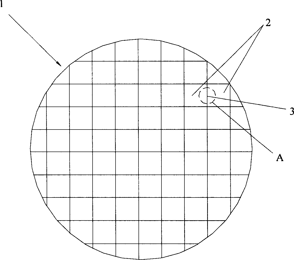
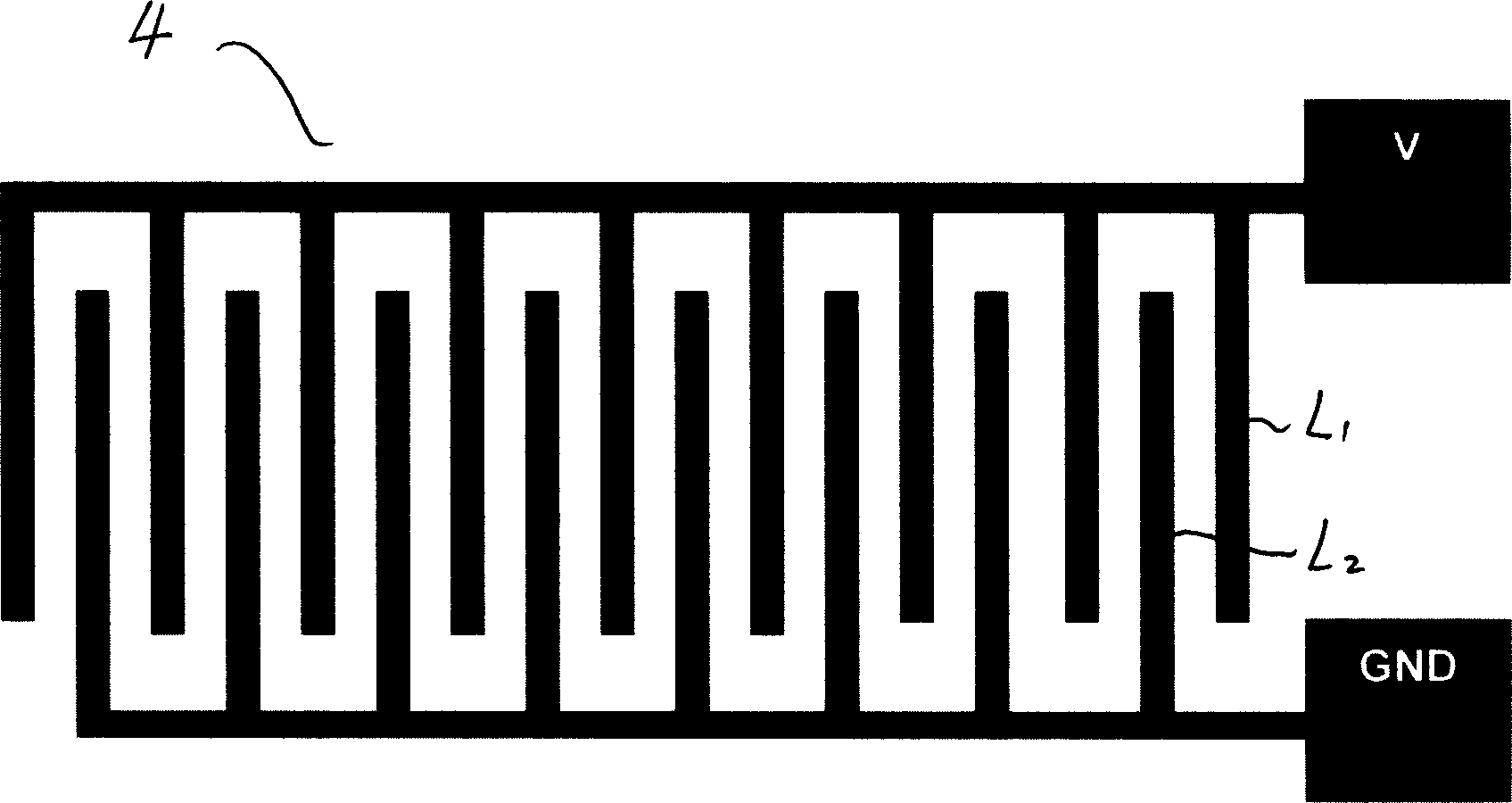
[0013] like figure 1 , figure 2 As shown, the present invention provides a method for on-line reliability testing of metal interconnects in a wafer. The method is to use the comb-shaped circuit of the test circuit 4 on the scribe line 3 between the main circuits (Circuit) 2 on the wafer 1 to apply a test voltage (Voltage), and measure Connection l in comb circuit 1 with connection l 2 Leakage Current and gradually increase the test voltage (Voltage), if the measured leakage current is small and its magnitude remains basically unchanged with the increase of the test voltage (the measured leakage current is in a small range) , indicating that the reliability of the wafer metal interconnects is good.

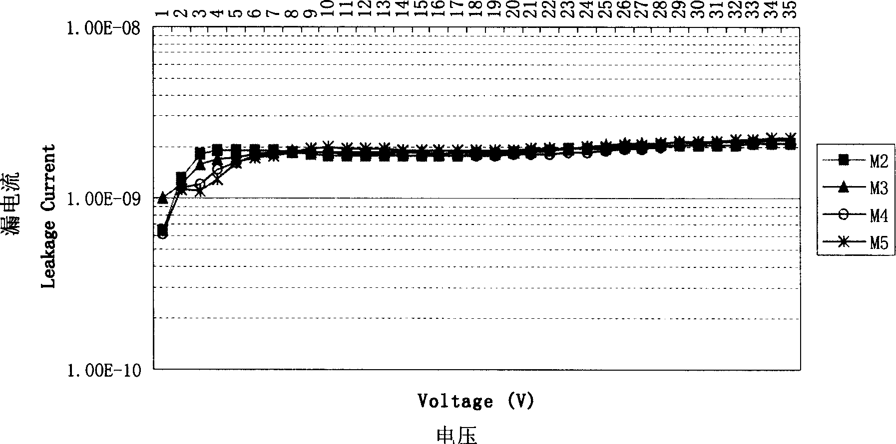
[0014] see image 3 , which shows a schematic diagram of the electrical test results of a 5-layer Cu metal interconnection of a wafer. As shown in the figure, the comb-shaped circuit of the test circuit applies a test voltage (Voltage), which increases by 1v each time, from 0v...


PUM


Abstract

This invention provides a transistor metal connection wire reliability on line test method, which comprises the following steps: using the transistor cutting channel test circuit and exerting test voltage on any point of the test circuit comb circuit; testing the leakage current between the connection wires of the comb circuit; step by step increasing the test voltage, if the leakage current tested is small and the voltage is basically stable, which means the metal transistor connection wire electric characteristic has good reliability, otherwise, there is some problems existing.

Description

technical field [0001] The invention relates to a method for detecting electrical characteristics of a chip, in particular to an on-line test of the reliability of a metal interconnection wire of a chip. Background technique [0002] With the shrinking of the size of integrated circuits and the increase in the area of ​​silicon wafers, the integrated circuit industry has stepped into the scope of 0.13mm line width technology, and the circuit complexity or integration of integrated circuits has increased, requiring multiple layers of polysilicon layers; On the one hand, the line width of the metal line cannot be reduced according to the reduction ratio of the MOS device, so the previous design of a single metal layer can no longer complete the wiring work of the entire integrated circuit, and must use 2 layers, 3 layers or more. Layers of metal interconnect lines to meet the requirements of circuit design. When there is a need for the above multi-layer polysilicon and multi-...

Claims


Application Information

Patent Timeline
Patent Type & Authority Applications(China)
IPC IPC(8): H01L21/66
CPCH01L2924/0002
Inventor 姜庆堂陈星星李鹤鸣
Owner SEMICON MFG INT (SHANGHAI) CORP
Why Eureka
Try Eureka