Method for deactivation of semiconductor laser cavity surface

A technology of lasers and semiconductors, applied in the direction of superimposed layer plating, ion implantation plating, coating, etc., can solve the problems of high cost, complicated process, and demanding equipment, and achieve stable performance, simple process, and low cost. effect of difficulty

Inactive Publication Date: 2005-09-21
BEIJING UNIV OF TECH
View PDF0 Cites 10 Cited by
  • Summary
  • Abstract
  • Description
  • Claims
  • Application Information

AI Technical Summary

Problems solved by technology

Although this method can better improve the reliability of the device, it h

Method used


Image

  • Method for deactivation of semiconductor laser cavity surface

Examples


Embodiment Construction

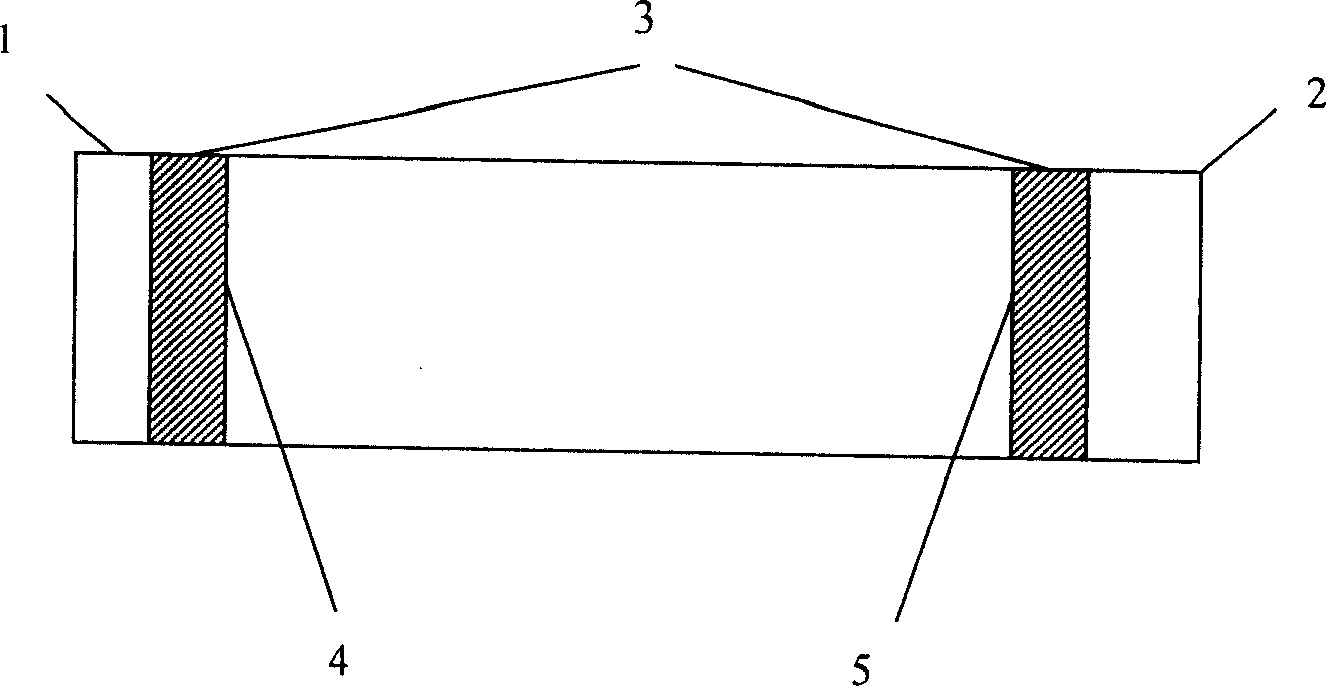
[0021] (1) After the semiconductor laser is cleaved into strips in the air, it is loaded into a special fixture for coating, and then placed in an electron beam evaporation vacuum chamber;

[0022] (2) Ion pre-cleaning: Ar or other ion sources with little damage can be selected; ion pre-cleaning is carried out on the front cavity surface 4 of the semiconductor laser for 30 seconds or 3 minutes or 6 minutes;

[0023] (3) Evaporating ZnSe or ZnS wide-bandgap low-absorption material on the front cavity surface 4 by electron beam evaporation as a passivation barrier layer 3 to prevent the diffusion of oxygen and impurities in the cavity surface mirror medium to the cavity surface;

[0024] (4) Anti-reflection coating 1 is plated on front chamber surface 4 according to prior art;

[0025] (5) After the fixture is turned over, the back cavity surface 5 is processed, and the above step (2) is carried out on the semiconductor laser back cavity surface 5;

[0026] (6) Evaporation of Z...


PUM


Abstract

The invention belongs to the semiconductor laser field. It comprises the following steps: cleaving the semiconductor laser to ropes in the air, then loading a fixture and putting it into an electron-beam vapor vacuum chamber; ion precleaning, that is to remove the oxidant and impurity substance in the cleaved cavity surface and the non-radiative recombination center as formed surface state and interface state with low energy ion current, which is less than 100eV , in the air of the electron-beam vapor vacuum chamber; ion precleaning the front cavity surface(4) for 30 seconds to 6 minutes; depositing broad forbidden band low absorbing material such as ZnSe or ZnS on the front cavity surface(4) to be an inactivating blocking layer(3) in the way of electron-beam vapor deposition; plating reflection reducting coating(1) on the front cavity surface(4); ion precleaning the rear cavity surface(5) from the back of the fixture for 30 seconds to 6 minutes; depositing ZnSe or ZnS on the rear cavity surface(5) in the way of electron-beam vapor deposition; plating high negative coating(2) on the rear cavity surface(5). The invented inactivating film is of stable performance, improved reliability, simple preparation, which can be used in lasers with different wave lengths or structures.

Description

1. Technical field [0001] The invention relates to a method for passivating the cavity surface of a semiconductor laser, which is suitable for various semiconductor ridge waveguide lasers and wide strip lasers with different wavelengths. 2. Background technology [0002] Semiconductor lasers are core devices in the fields of optical communication, optical pumping, and optical storage. Due to the influence of the interface state, impurity contamination or strain on the cavity surface, the light absorption is enhanced, and the temperature rises sharply, which in turn enhances the light absorption, and it is easy to oxidize and produce defects, which makes the laser performance decline and optical catastrophe occur. Sexual damage, which is particularly prominent for high-power lasers. In order to reduce the influence of these factors and improve the reliability of the laser, the cavity surface of the laser is usually coated. Generally, this coating not only protects the cavit...

Claims


Application Information

Patent Timeline
IPC IPC(8): C23C14/24C23C28/00
Inventor 徐晨沈光地舒雄文田增霞陈建新高国
Owner BEIJING UNIV OF TECH
Why Eureka
Try Eureka