UV laser drilling hole method

A technology of laser drilling and laser beam, which is applied in the direction of removing conductive materials by mechanical methods, can solve problems such as cracking and falling off of the electroplating layer, fracture of the electroplating copper layer, and poor electroplating, so as to increase processing flexibility and improve processing Quality, simple effect of optical path system

Inactive Publication Date: 2005-09-28
HANS LASER TECH IND GRP CO LTD +1
View PDF0 Cites 23 Cited by
  • Summary
  • Abstract
  • Description
  • Claims
  • Application Information

AI Technical Summary

Problems solved by technology

[0008] Microvias with these quality problems will have serious hidden dangers in subsequent processing and use. If insulating materials remain at the bottom of the holes, after the holes are electroplated with copper, there will be gaps between the electroplated copper layer and the inner copper pattern layer. The insulating layer is very easy to cause electrical disconnection, even if there is less residue and electrical conduction, but due to the small area of ​​contact between the electroplated copper layer and the inner copper pattern layer, the adhesion strength is poor, in the s

Method used


Image

  • UV laser drilling hole method
  • UV laser drilling hole method
  • UV laser drilling hole method

Examples


Embodiment Construction

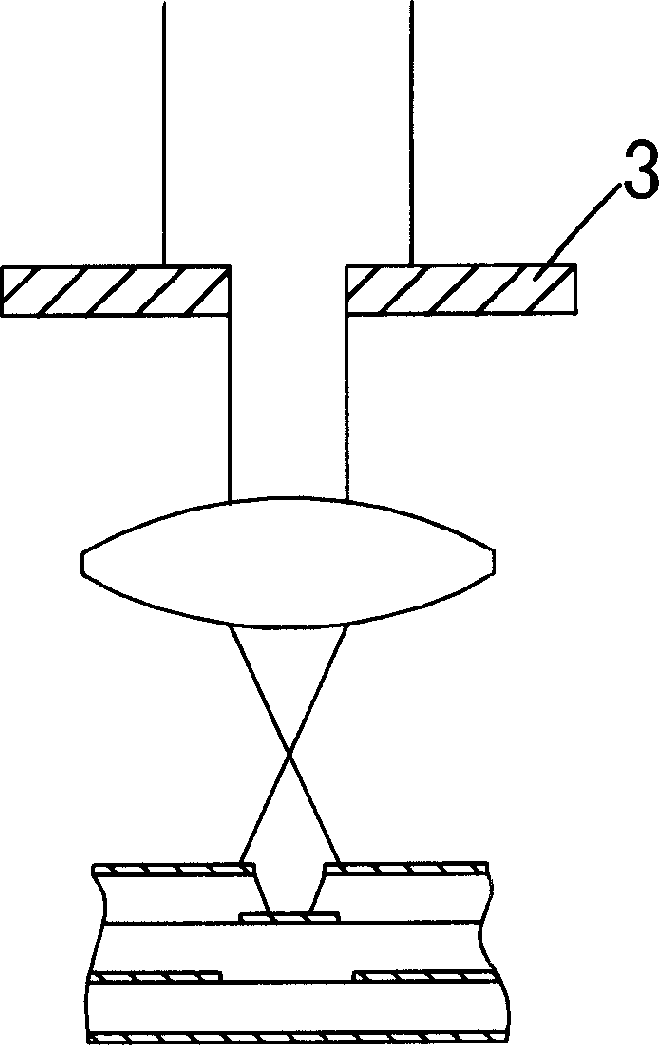
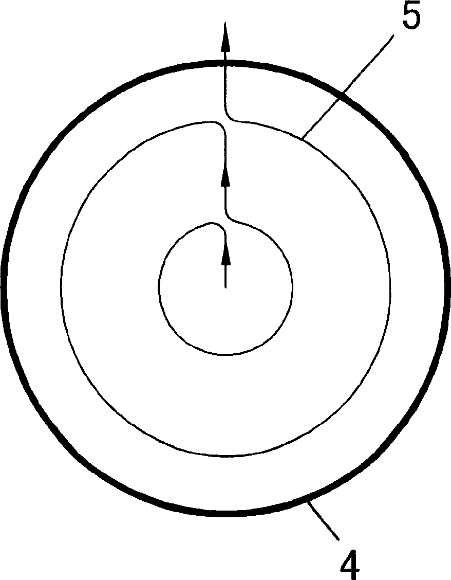
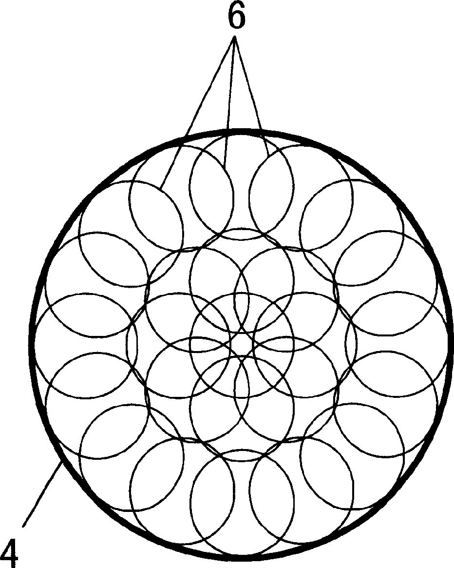
[0021] see Figure 3a , Figure 3b , Figure 4 , Figure 5a , Figure 5b and Figure 6 , the present invention adopts the method of UV laser drilling to process the micro via hole 4 on the high-density interconnection printed circuit substrate. As we all know, the wavelength of UV laser is very short (less than 400nm), the energy density after focusing is extremely high, and most materials have a relatively high absorption rate for UV laser. After absorbing UV laser, various materials will destroy the molecular bonds of organic matter, metals, etc. The metal bond of the crystal and the ionic bond of the inorganic matter make it form suspended particles or atoms, molecular groups, etc. to escape, thereby forming a blind hole for connectivity between the inner and outer copper pattern layers of the multilayer printed circuit board. After the hole wall is cleaned and copper-plated, the copper pattern layer 1 of the inner layer and the outer layer can be connected together to...


PUM


Abstract

The present invention relates to an UV laser drilling method for making microconductive through-hole one printed circuit base board. Said method includes the following steps: utilizing UV laser beam to scan the position having need of making microconductive through-hole along a certain pathway, then successively making several microholes until the area of whole surface around the microconductive through-hole in covered with the made microholes all over, and then carving the whole microconductive through-hole. Said invention adopts the ring sawing process, so that it can raise the making quality of the microconductive through-hole.

Description

Technical field [0001] The invention relates to a method for laser drilling on a printed circuit substrate, in particular to a method for using UV laser drilling. Background technique [0002] With the miniaturization and portability of electronic equipment, there is an increasing demand for higher circuit density on printed circuit boards. To adapt to the above requirements, in recent years, a laminated multilayer printed circuit board with a higher density conductive layer (generally 2 to 4 layers) sequentially laminated on one or both sides of a conventional high-density printed circuit board has appeared. The board has smaller microvias, thinner insulation layer thickness and finer and shorter line width / spacing. Between the upper and lower printed circuit boards in the above-mentioned multilayer printed circuit board, it is necessary to electrically connect the conductive layer, wherein the conductive layer is generally composed of a copper pattern (pattern), and the i...

Claims


Application Information

Patent Timeline
IPC IPC(8): H05K3/04
Inventor 李强周建辉
Owner HANS LASER TECH IND GRP CO LTD
Why Eureka
Try Eureka