
Local medium thickening method for improving silicon integrated inductance quality factor

A technology integrating inductance and quality factor, which is applied in the direction of circuits, electrical components, fixed transformers or mutual inductance, and can solve problems such as complex processes

Inactive Publication Date: 2005-11-02
INST OF MICROELECTRONICS CHINESE ACAD OF SCI
View PDF0 Cites 0 Cited by
  • Summary
  • Abstract
  • Description
  • Claims
  • Application Information

AI Technical Summary

Problems solved by technology

The most widely reported method is to use micromechanical system (MEMS) technology to hollow out the silicon substrate below the inductor (for representative literature, see J.Y C. Chang, A.A. Abidi and M. Gaitan, "Largesuspended inductors on silicon and their use in a 2mm CMOS RF amplifier," IEEE Electron Device Letters, Vol.14, May 1993, pp246-248.), although it can improve the quality factor of the inductor, it is not only complicated in process, but also has long-term reliability problems

Method used


Image

  • Local medium thickening method for improving silicon integrated inductance quality factor

Examples


Embodiment Construction

[0016] The present invention is a local medium thickening method for improving the quality factor of silicon integrated inductance, comprising the following steps:

[0017] Step 1: Deposit silicon dioxide / silicon nitride / silicon dioxide three-layer composite dielectric; this step 1 uses the deposition method to grow silicon dioxide / silicon nitride / silicon dioxide three-layer composite dielectric, and the three-layer dielectric The thickness ranges are 15-30nm, 50-100nm, 500-3000nm in turn.

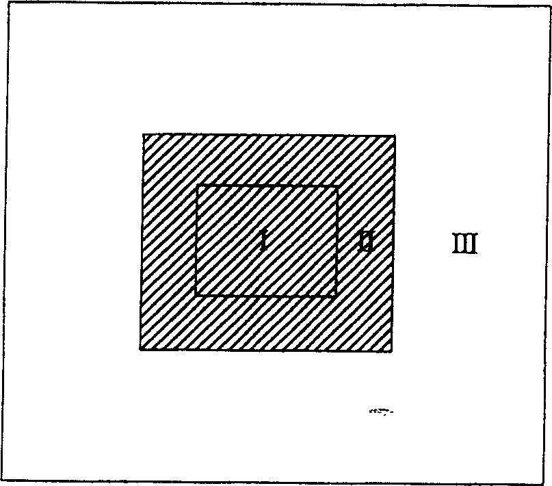
[0018] Step 2: The photoresist protects the area of ​​the spiral inductor and exposes the area outside the plane of the spiral inductor; this step 2 uses the photoresist to protect the planar spiral inductor and the area within 5 microns around it; as figure 1 As shown, area I (the rectangle with the smallest area in the center of the figure) is the planar area of ​​the spiral inductor, area II (the shaded area, including area I) is the photoresist protection area, and area III (the area o...


PUM


Abstract

A method for improving the quality factor or the silicon integrated inductor and thickening the partial medium is characterized in that it comprises the steps of: depositing three-layer composite medium of silicon dioxide / silicon nitride / silicon dioxide; photo resisting protection of the spiral inductor area and the area exposed on the outside of the spiral inductor flat; wet corroding the top layer silicon dioxide, dry etching silicon nitride and bottom layer silicon dioxide; striping and cleaning.

Description

technical field [0001] The invention belongs to the technical field of semiconductors, in particular to a local dielectric thickening technology for improving the quality factor of silicon (Si) integrated inductance. Background technique [0002] In recent years, with the rapid development of wireless communication technology, the market demand for radio frequency integrated circuits (RFIC) has increased dramatically. Due to the advantages of low cost, low power consumption and easy integration of radio frequency (RF) complementary metal oxide semiconductor (CMOS) technology, major companies, universities and research institutions are competing to join in the research and development. Si RFICs are challenging or replacing traditional gallium arsenide (GaAs) technology in certain application fields, and are regarded as the future trend of RFIC development. The planar spiral inductor is a very important passive component in RFIC, and its quality factor determines or affects t...

Claims


Application Information

Patent Timeline
Patent Type & Authority Applications(China)
IPC IPC(8): H01L21/02
Inventor 李俊峰杨荣李力南扈焕章蒋浩杰白国斌钱鹤
Owner INST OF MICROELECTRONICS CHINESE ACAD OF SCI
Learn More