Differential amplifier in low voltage and low power consumption and high isolation

A differential amplifier, high isolation technology, applied in differential amplifiers, DC-coupled DC amplifiers, improved amplifiers to reduce noise effects, etc., can solve problems such as poor isolation effect, circuit stability problems, and application difficulties, and reduce power consumption. Effect of voltage and power consumption, high isolation, and strong application prospects

Inactive Publication Date: 2005-11-16
PEKING UNIV
View PDF0 Cites 9 Cited by
  • Summary
  • Abstract
  • Description
  • Claims
  • Application Information

AI Technical Summary

Problems solved by technology

However, because only a single tube is used, the isolation effect between the input and output terminals will become very poor due to the Miller effect, so the application range of this structure is limited in the actual application process.
Especially the application at high frequency is more difficult, because it will make the stability of the circuit a big problem

Method used


Image

  • Differential amplifier in low voltage and low power consumption and high isolation
  • Differential amplifier in low voltage and low power consumption and high isolation
  • Differential amplifier in low voltage and low power consumption and high isolation

Examples


Embodiment Construction

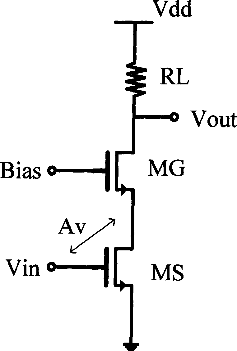
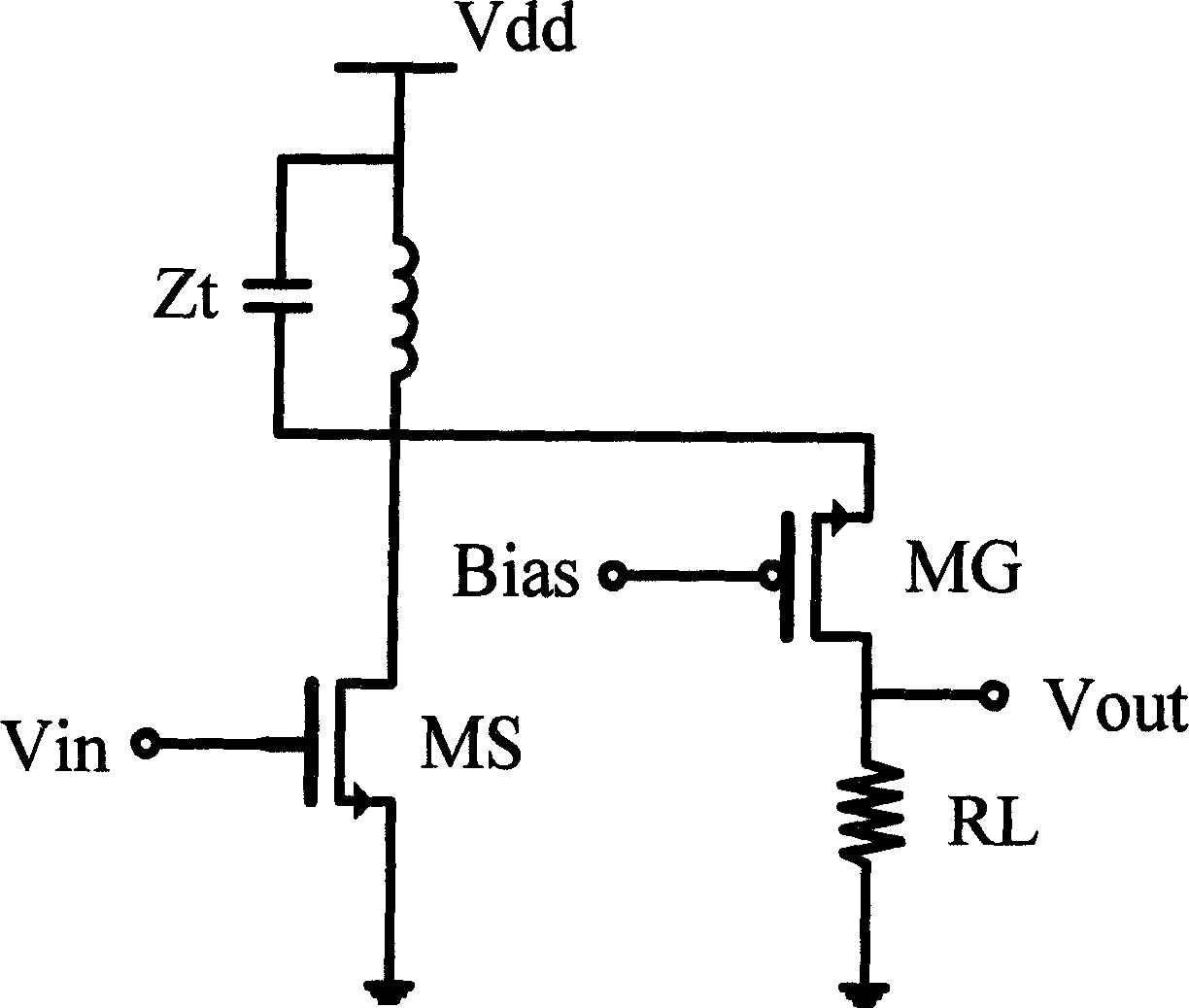
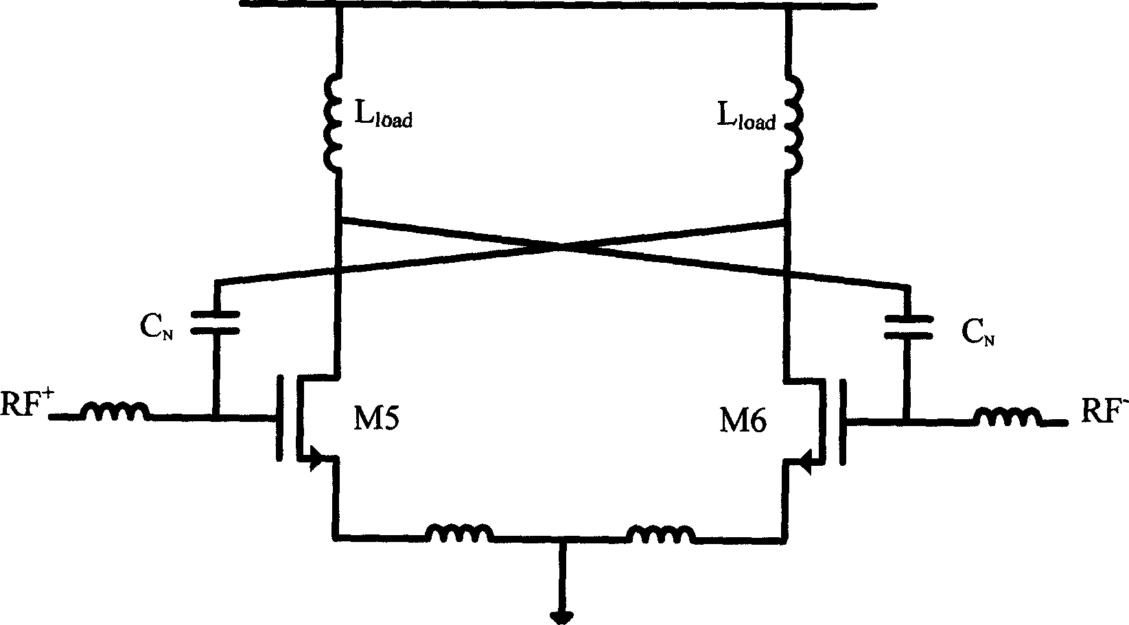
[0020] The low-voltage, low-power consumption and high-isolation differential amplifier of the present invention uses two MOSFETs connected in a common source mode as the input terminals of two differential signals, uses resistors, inductors or other active devices as loads, and uses resistors, inductors or other active The device is used as the feedback element or tail current source of the amplifier source; at the same time, two MOSFETs that are identical to the input MOSFET are used. The gate terminal of the MOSFET is connected to the drain terminal of the common source MOSFET that inputs the negative signal (negative output terminal), the gate terminal of the other MOSFET is connected to the gate terminal of the common source MOSFET that inputs the negative signal, and the drain terminal of the MOSFET The terminal is connected to the drain terminal of the common source MOSFET that inputs the positive signal (positive output terminal) in a cross-connection manner. The load ...


PUM


Abstract

Two MOSFETs connected in common source mode are as input ends of the differential signal of amplifier. Resistance, inductance or other active device is adopted as load as well as feedback element at source end of amplifier or trail current source. Two MOSFETs identical to two input MOSFETs in common source mode are added. Gate end of one MOSFET is connected to gate end of input MOSFET for inputting positive signal; and drain end is connected to drain end of input MOSFET for inputting negative signal (negative output end). Gate end of the other MOSFET is connected to gate end of input MOSFET for inputting negative signal; and drain end is connected to drain end of input MOSFET for inputting positive signal (positive output end). The invention takes full advantage of identical gate-drain capacitances of MOSFET parts operated at saturation region and cutoff region. Features are: low voltage, low power consumption and high degree of reverse isolation.

Description

technical field [0001] The invention belongs to the application technical field of low-voltage and low-power CMOS RFIC in the deep submicron era, and is especially suitable for a low-noise amplifier (LNA) in a radio frequency CMOS integrated circuit (RFIC). Background technique [0002] As CMOS VLSI technology enters the era of 65nm technology, the field effect transistor in the circuit has a serious short channel effect, which is manifested by the decrease of the threshold voltage (threshold voltage) as the channel length decreases. The threshold voltage decreases with the increase of the drain terminal voltage, and the intrinsic output resistance of the device is reduced due to the direct source-drain punch-through (punch-through) channel length modulation effect. The second-order effect of the device caused by the short channel effect is easy to cause circuit failure. Therefore, the suppression of short-channel effects is an urgent problem to be solved to improve the per...

Claims


Application Information

Patent Timeline
Patent Type & Authority Applications(China)
IPC IPC(8): H03F1/26
Inventor 宋睿丰廖怀林张国艳
Owner PEKING UNIV
Why Eureka
Try Eureka