

Plane button type packing technology of integrated circuit or discrete component and its packing structure
A planar bump type, discrete component technology, applied in the direction of electrical components, circuits, electrical solid devices, etc., can solve the problems affecting solderability, air residue, water absorption rate increase, etc., to achieve reliability assurance and stable quality , Yield rate improvement effect
- Summary
- Abstract
- Description
- Claims
- Application Information
AI Technical Summary
Problems solved by technology
Method used
Image


Examples
Embodiment Construction
[0058] The integrated circuit or discrete component planar bump type packaging process of the present invention consists of the following procedures:
[0059] 1) Substrate - see figure 1 , take a piece of metal substrate 1 with an appropriate thickness. The material of the metal substrate 1 can be changed according to the functions and characteristics of the chip, for example: nickel-iron alloy, pure copper or copper alloy.
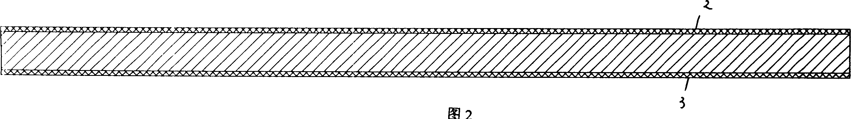
[0060] 2) Paste dry film—see Figure 2, paste dry film layers 2 and 3 on the front and back sides of the metal substrate to protect the subsequent etching process.
[0061] 3) Remove the upper part of the dry film - see image 3 , remove the dry film on the upper layer of the metal substrate 1, and prepare to form base islands and pins on the metal substrate 1, in order to expose the area on the upper layer of the substrate that needs to be metallized later.
[0062] 4) Metallized layer on the substrate - see Figure 4 , plate the required metal layer...
PUM
 Abstract
Description
Claims
Application Information