Light-emitting diode device and production method thereof

A technology of light-emitting diodes and devices, which is applied to semiconductor devices, electrical components, circuits, etc., and can solve problems such as blocking and emission efficiency reduction

Inactive Publication Date: 2006-04-12
SHOWA DENKO KK
View PDF5 Cites 8 Cited by
  • Summary
  • Abstract
  • Description
  • Claims
  • Application Information

AI Technical Summary

Problems solved by technology

[0024] However, in the light emitting device disclosed in JP-A 2001-189493, although the distributed electrodes are dispersed and have a small area, the light emitted in the area directly under each electrode is extracted from the upper part of the light emitting device by electrode barrier
It was found that such blocking causes a decrease in the emission efficiency

Method used


Image

  • Light-emitting diode device and production method thereof
  • Light-emitting diode device and production method thereof
  • Light-emitting diode device and production method thereof

Examples


Embodiment Construction

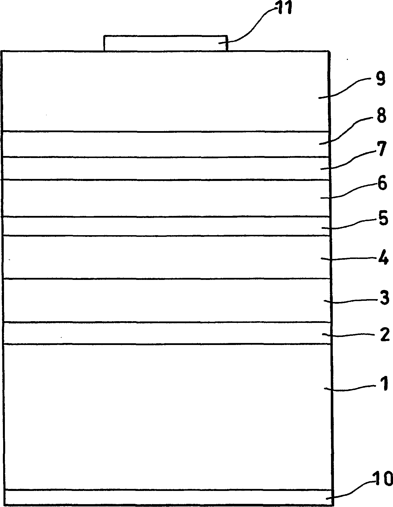
[0068] figure 1 is a schematic cross-sectional view showing one embodiment of a double heterostructure light emitting diode (LED) device with an AlGaInP active layer according to the present invention. In this embodiment, a buffer layer 2, a reflective layer 3, an n-type cladding layer 4, a first undoped AlInP layer 5, an active layer 6, a second undoped AlInP layer 7, p-type intermediate layer 8 and window layer 9 , while providing n-electrode 10 on the back surface of substrate 1 and p-electrode 11 on the front surface of window layer 9 .

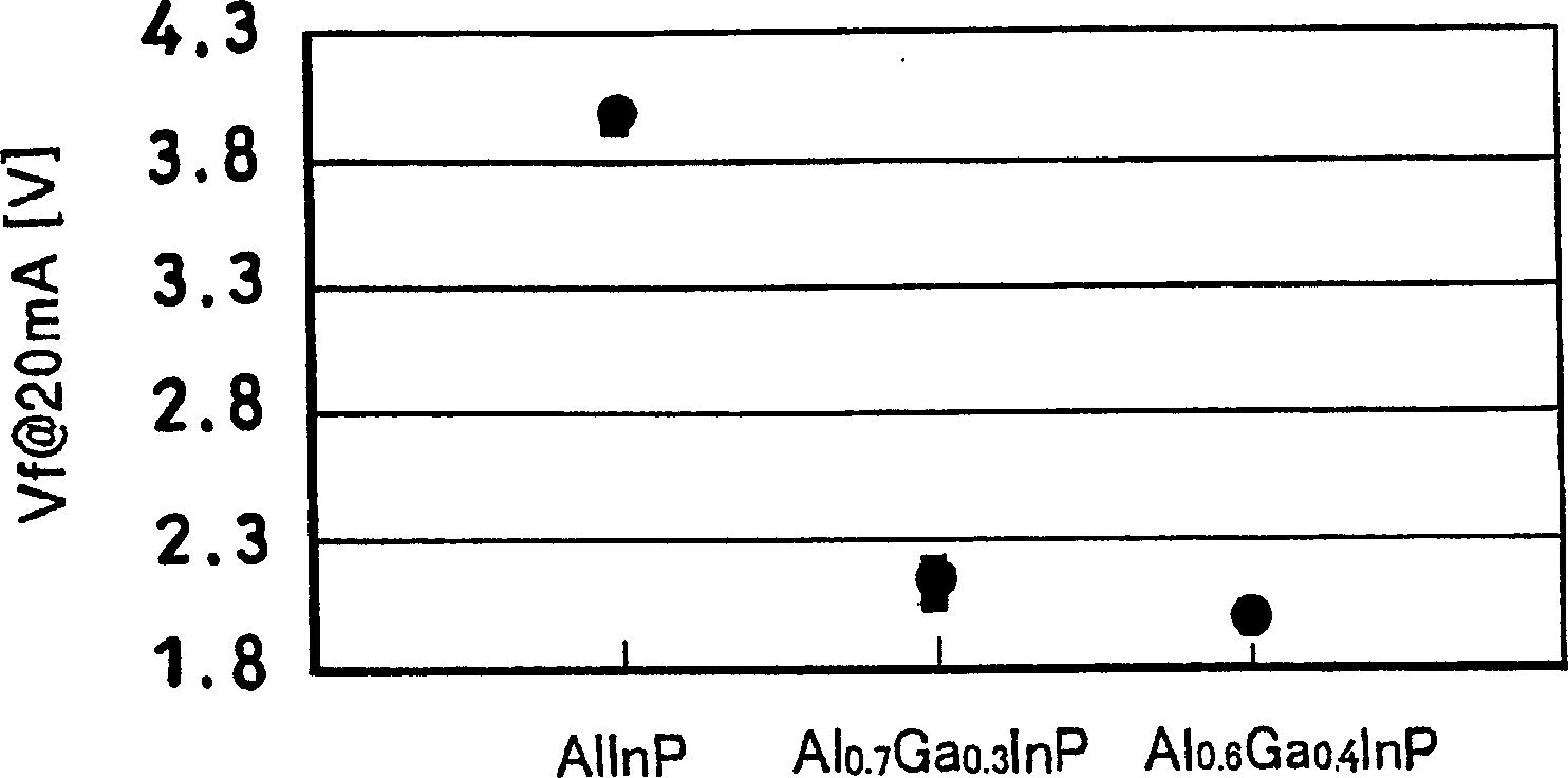
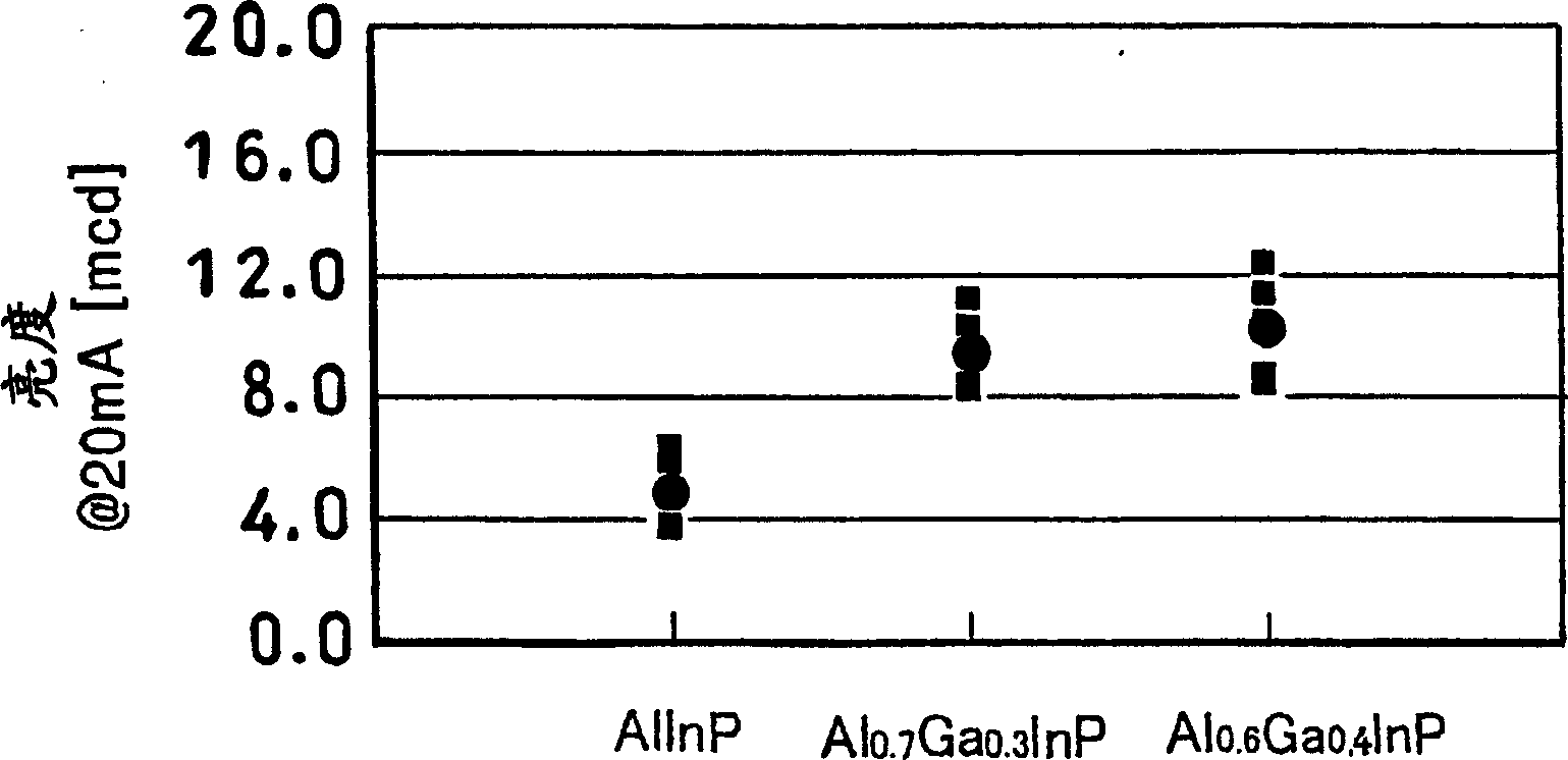
[0069] The substrate used in this embodiment was a silicon (Si) doped gallium arsenide (GaAs) substrate (15° offset from (100)). On the substrate, by using trimethylgallium (Ga(CH 3 ) 3 ), trimethylindium (In(CH 3 ) 3 ), trimethylaluminum (Al(CH 3 ) 3 ), dimethyl zinc (Zn(CH 3 ) 2 ), disilane (Si 2 h 6 ), arsenic trihydride (AsH 3 OO) and phosphine (PH 3 ) to form the layers listed in Table 1 below. Note that during film fo...


PUM


Abstract

A double hetero structure light-emitting diode device includes an active layer ( 6 ), a positive-electrode-side cladding layer, a negative-electrode-side cladding layer ( 4 ), a window layer ( 9 ) and an undoped AlInP layer. The positive-electrode-side cladding layer includes an undoped AlInP layer ( 7 ) grown to have a thickness of 0.5 mum and an intermediate layer ( 8 ) doped to assume p-type conductivity and having an intermediate energy band gap value between that of the undoped AlInP layer and that of the window layer. The window layer on the intermediate layer is a GaP layer grown at 730 DEG C. or higher and at a growth rate of 7.8 mum/hour or more in the presence of Ze serving as a dopant. The negative-electrode-side cladding layer is provided with an undoped AlInP layer ( 5 ) having a thickness of 0.1 mum or more. With this configuration, there is provided a light-emitting diode device that enhances the crystallinity of a window layer, prevents generation of faults caused by a high-temperature process and attains high luminance at a wavelength falling within a yellow-green band.

Description

[0001] Cross References to Related Applications [0002] This application is based upon an application filed under 35 U.S.C. §111(a) pursuant to 35 U.S.C. §119(e)(1), requiring a provisional application filed under 35 U.S.C. §111(b) on February 20, 2003 Priority of Provisional Application No. 60 / 448,104 and Provisional Application No. 60 / 456,561, filed March 24, 2003. technical field [0003] The present invention relates to a light emitting diode (LED) device emitting visible light and to a method for manufacturing the LED device. Background technique [0004] Find various uses of LEDs including displays. As is well known, the emission wavelengths of LEDs using semiconductors depend on the type of semiconductors and increase in the order of InGaN, AlGaInP, GaAlAs, and GaInAsP. The brightness of LEDs is increasing year by year, and high-brightness LEDs are now used as lighting devices or as backlights for liquid crystal displays. However, research to further increase brig...

Claims


Application Information

Patent Timeline
Patent Type & Authority Applications(China)
IPC IPC(8): H01L33/00H01L33/06H01L33/10H01L33/14H01L33/30H01L33/38H01L33/42
Inventor 竹内良一松泽圭一山崎润一
Owner SHOWA DENKO KK
Why Eureka
Try Eureka