Warm-up flash two-purpose nano impression device

A nano-imprinting, dual-purpose technology, applied in the direction of photolithography process exposure device, micro-structure device, manufacturing micro-structure device, etc. And the effect of strong practicability and wide application range

Inactive Publication Date: 2006-05-24
INST OF OPTICS & ELECTRONICS - CHINESE ACAD OF SCI
View PDF0 Cites 14 Cited by
  • Summary
  • Abstract
  • Description
  • Claims
  • Application Information

AI Technical Summary

Problems solved by technology

Both have their own advantages and disadvantages. The former can be used for large-area imprinting, but it needs to be heated at high temperature and high pressure, and at the same time, the temperature must be lowered below the glass temperature of the polymer, etc.; High temperature and high pressure

Method used


Image

  • Warm-up flash two-purpose nano impression device
  • Warm-up flash two-purpose nano impression device
  • Warm-up flash two-purpose nano impression device

Examples


Embodiment Construction

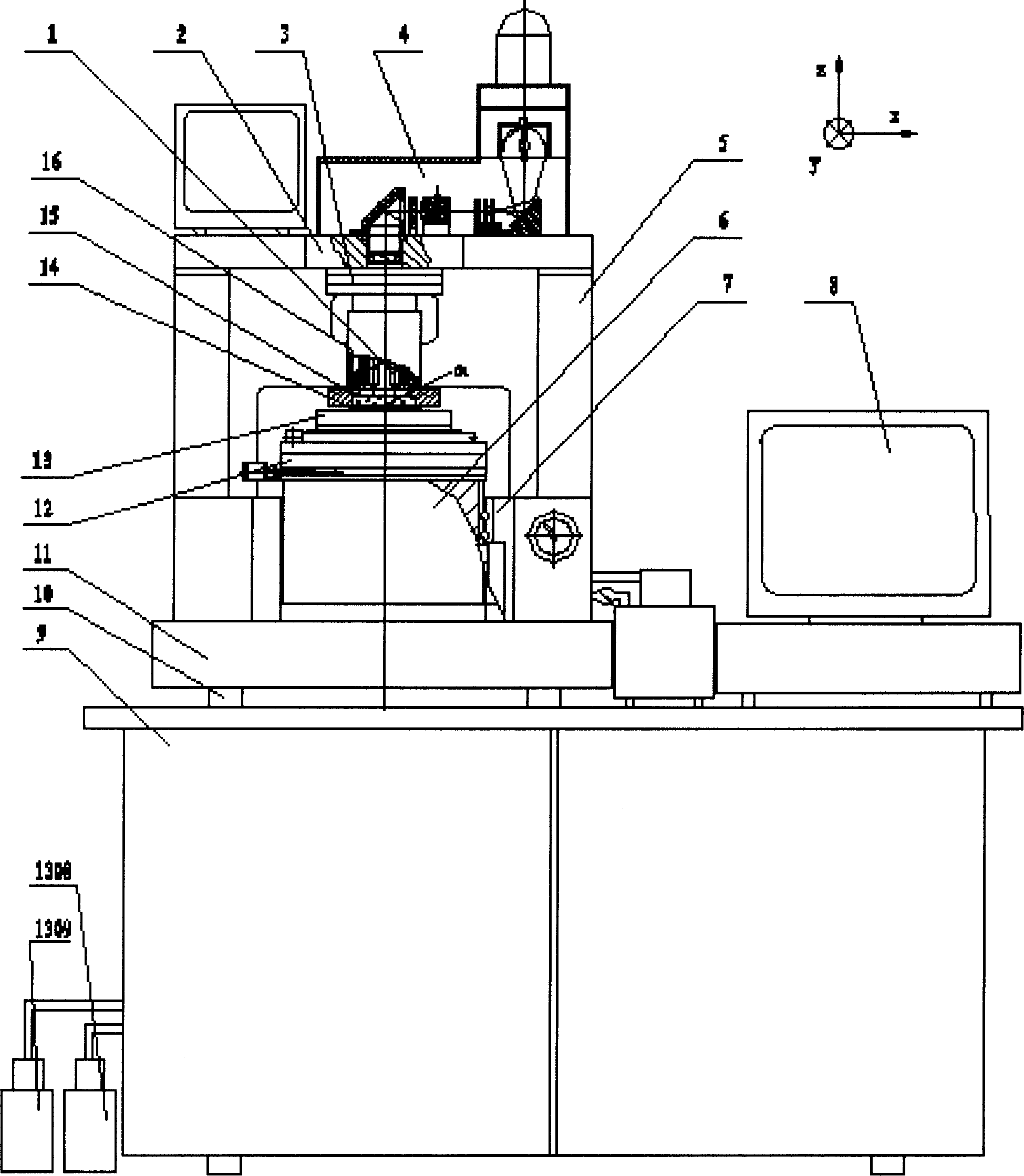
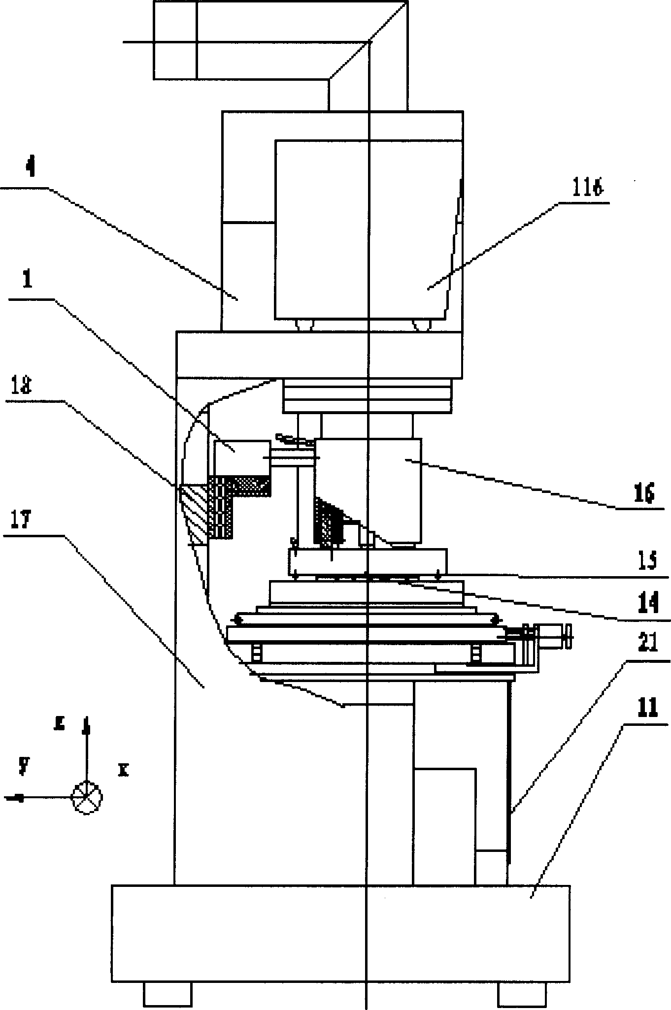
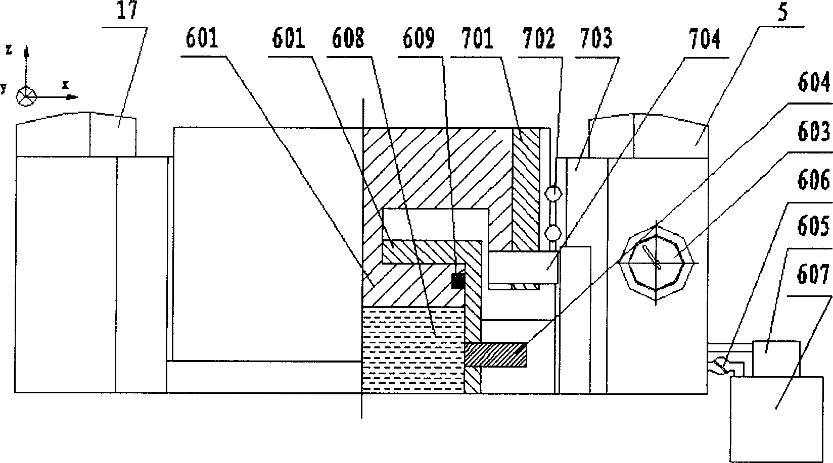
[0034] Such as figure 1 , 2 As shown, the embodiment of the present invention consists of a dual-channel CCD alignment system 1, a horizontal plate 2, a Z-direction corrector 3, a purple light illumination system 4, a left side plate 5, a right side plate 17, a rear plate 18, and an oil pressure jacking system 6 , Z-direction linear guide rail mechanism 7, computer system 8, machine cabinet 9, main machine base plate 11, XYθ micro-motion workpiece table 12, substrate heating table 13, substrate 14, die 15, tilt calibration mechanism 16 and control system 20 and other parts. The large base plate 11 of the main machine is placed on the table top of the machine cabinet 9 through the vibration isolation pad 10, and the electrical control system 20 placed in the machine cabinet 9 has an embossing control 201, a CCD image and A / D conversion circuit 202, and an XYθ micro-motion workpiece The measurement drive control circuit 203, constant light intensity and integral shutter contro...


PUM


Abstract

The stamping apparatus is composed of CCD alignment system in two way, corrector in Z direction, illumination system in purple light, left and right side plates, oil pressure lifting jack system, heating desk for loaded piece, slant correcting mechanism and control system. Large base plate of host is on equipment cabinet. The large base plate, left and right side plates, backboard and upper transverse plate constitute frame. Corrector in Z direction and slant correcting mechanism with press mold are hung underside of the transverse plate. Oil lifting jack system faced to the press mold is installed at middle. XYtheta micromotion work desk, the heating desk, substrate is lifted by jack system to impact the mold to stamp out Nano graph structure. Illumination system in purple light illumines polymer in stamping layer to solidify it. Heating up and cooling down heating desk solidifies and demoulds the polymer. The invention possesses advantages of two stamping methods.

Description

technical field [0001] The invention is a dual-purpose nano-imprinting device for heating and flashing, which belongs to the field of nano-graphic structure devices produced by micro-processing technology. Background technique [0002] Due to the high-speed development of high-tech information technology, microfabrication technology is urgently required to produce ultra-high-speed, ultra-high-frequency nanoscale IC devices, and the production of nano-graphic structures requires a substantial increase in the resolution of existing lithography. Generally, methods of shortening wavelength lithography are used, such as deep ultraviolet lithography, extreme ultraviolet lithography, X-ray lithography, ion beam projection lithography, and electron beam lithography. They all require an extremely short-wavelength light source electromagnetic radiation system and an optical system, which are not only technically complex, but also very expensive to invest. [0003] At present, new tec...

Claims


Application Information

Patent Timeline
IPC IPC(8): G03F7/00B41M5/26B81C1/00G03F7/20G03F9/00
Inventor 罗先刚陈旭南胡承刚
Owner INST OF OPTICS & ELECTRONICS - CHINESE ACAD OF SCI
Why Eureka
Try Eureka