Method and apparatus for preventing metal/silicon spiking in MEMS devices

A technology of micro-electromechanical structure and silicon layer, which is applied in metal material coating process, microstructure technology, microstructure device, etc., can solve problems such as increased resistivity of aluminum wire, difficulty in dry etching of alloy aluminum wire, and wrong operation of components.

Inactive Publication Date: 2006-05-31
TAIWAN SEMICON MFG CO LTD
View PDF2 Cites 7 Cited by
  • Summary
  • Abstract
  • Description
  • Claims
  • Application Information

AI Technical Summary

Problems solved by technology

However, this method also has disadvantages. In addition to causing a slight increase in the resistivity of the aluminum wire, it will also cause difficulties in the dry etching of the alloy aluminum wire (because copper is not easy to produce highly volatile fluoride or chloride, and silicon is still in aluminum. will coalesce and increase the difficulty of dry etching)
[0006] Therefore, for some special processes, especially the micro-electromechanical (Surface MEMS) process in which silicon is filled between aluminum metal patterns as a sacrificial layer (Sacrificial layer), such as Figure 1A As shown, it is a schematic diagram of a partial structure of an optical micro-electromechanical system. A substrate 100 includes a plurality of aluminum metal patterns, and an amorphous silicon layer 106 is filled between and on the first aluminum metal pattern 102 and the second aluminum metal pattern 104. , the aluminum metal pattern 108 is used as a mirror (Mirror) to reflect the incident light wave, so the aluminum metal pattern 108 is a moving object, and accordingly changes the angle of the reflected wave to determine the transmission of the component signal, and therefore if In the subsequent filling of the amorphous silicon layer 106 and the aluminum metal pattern 108 in the spacer, because the temperature of the subsequent process exceeds about 370 ° C, the interdiffusion produces a spike phenomenon, such as Figure 1B As shown, in this way, the first aluminum metal pattern 102 and the second aluminum metal pattern 104 will be bridged (Bridging) together, and the operation of the device will also cause errors.

Method used


Image

  • Method and apparatus for preventing metal/silicon spiking in MEMS devices
  • Method and apparatus for preventing metal/silicon spiking in MEMS devices
  • Method and apparatus for preventing metal/silicon spiking in MEMS devices

Examples


no. 1 example

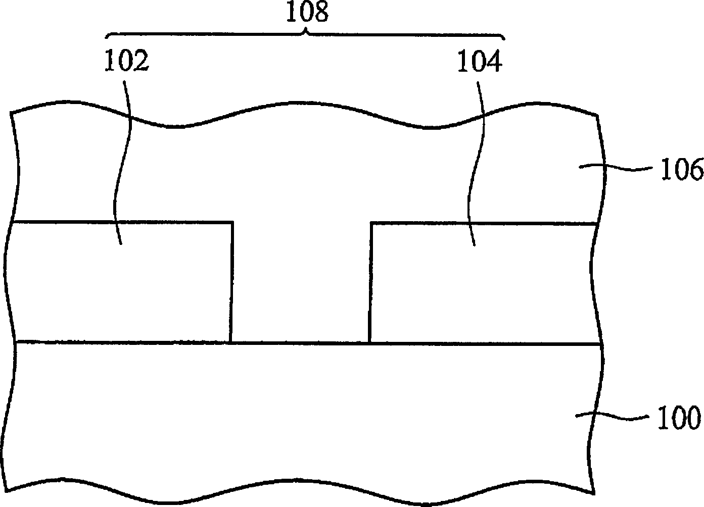
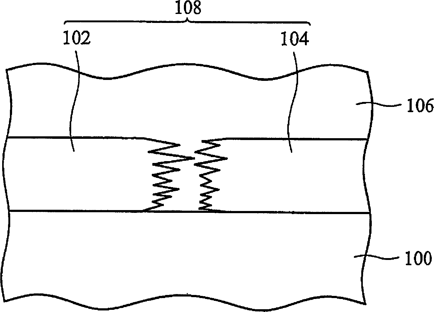
[0030] First, if Figure 2A As shown, a substrate 200 including a plurality of metal patterns 202 is provided, wherein the substrate 200 can be a semiconductor substrate or a glass substrate, and the metal patterns are composed of aluminum or a combination of aluminum, silicon, and copper. The preferred metal pattern 202 is an aluminum-silicon-copper alloy (about 1% silicon and 0.5% copper is added to the aluminum) with a thickness of 2000 angstroms to 4000 angstroms, which is deposited by sputtering and then etched back: its sputtering The method generally uses a high vacuum pump to reduce the pressure of the reaction formula to 10 -6 Below Torr, metal sputtering is then carried out in an environment with a pressure of about 1-10 mTorr by passing in an inert gas with a suitable atomic mass (generally argon). The etch back generally uses chlorides such as: SiCl 4 、BCl 3 、BBr 3 or CCl 4 Combination with chlorine gas for etching of aluminum.

[0031] The metal pattern also...

no. 2 example

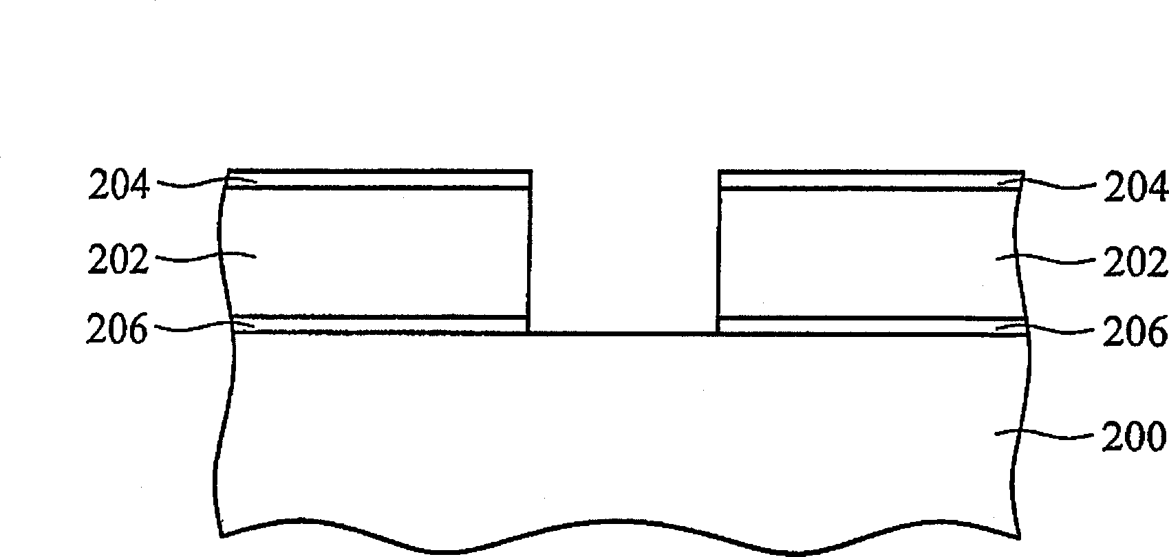
[0035] First, if Figure 3AAs shown, a substrate 300 including a plurality of metal patterns 302 is provided, wherein the substrate 300 can be a semiconductor substrate or a glass substrate, and the metal patterns 302 are composed of aluminum or a combination of aluminum, silicon, and copper. Its preferred metal pattern 302 is an aluminum-silicon-copper alloy (adding about 1% silicon and 0.5% copper to aluminum) with a thickness of 2000 angstroms to 4000 angstroms, which is deposited by sputtering and then etched back: its sputtering The method generally uses a high vacuum pump to reduce the pressure of the reaction formula to 10 -6 Below Torr, metal sputtering is then carried out in an environment with a pressure of about 1-10 mTorr by passing in an inert gas with a suitable atomic mass (generally argon). The etch back generally uses chlorides such as: SiCl 4 、BCl 3 、BBr 3 or CCl 4 Combination with chlorine gas for etching of aluminum.

[0036] Its metal pattern also in...


PUM

PropertyMeasurementUnit
thicknessaaaaaaaaaa
thicknessaaaaaaaaaa

Abstract

The invention provides a method and structure for preventing lateral interdiffusion between metal and silicon layers and a micro-electromechanical structure. The method includes the following steps: firstly, a substrate including a plurality of metal patterns is provided. Next, a silicon oxide layer, a silicon nitride layer, a silicon oxynitride layer, titanium nitride or aluminum oxide is formed on the spacer of the metal pattern to prevent the lateral interdiffusion between the metal pattern and the subsequent silicon layer.

Description

technical field [0001] The present invention relates to a micro-electromechanical or semiconductor process method and structure, in particular to a method and structure for preventing lateral cross-diffusion between metal and silicon layers in the micro-electromechanical process. Background technique [0002] The resistivity (Resistivity) of aluminum metal itself is quite low (about 3Ω-cm), and its adhesion to the silicon dioxide layer is good, and it is easy to be processed by dry etching based on chlorine (Cl), so Aluminum metal has been widely used as the main conductive material of components to reduce the RC time delay (Time Delay) and thereby increase the switching frequency of the components. [0003] Although aluminum has the advantages of low resistivity, good adhesion to the silicon dioxide layer, and easy processing of large-scale integrated circuits (VLSI), there are some problems that must be solved in practical applications: because silicon is in Aluminum has ...

Claims


Application Information

Patent Timeline
Patent Type & Authority Applications(China)
IPC IPC(8): B81B7/00B81C1/00H01L21/00
CPCB81C1/00253B81C2201/0178B81C2201/053
Inventor 张毓华陈斐筠曾健庭朱翁驹彭俊凯叶志杰柏竟衡何大椿
Owner TAIWAN SEMICON MFG CO LTD
Why Eureka
Try Eureka