Method for growing non-crack III family nitride on silicon substrate

A technology of nitride and silicon substrates, which is applied in the direction of electrical components, semiconductor/solid-state device manufacturing, circuits, etc., can solve the problems of not being able to introduce sufficient compensation for thermal tensile stress and compressive stress, and achieve low cost, weak dependence, and elimination of cracks Effect

Inactive Publication Date: 2006-08-30
INST OF SEMICONDUCTORS - CHINESE ACAD OF SCI
View PDF0 Cites 37 Cited by
  • Summary
  • Abstract
  • Description
  • Claims
  • Application Information

AI Technical Summary

Problems solved by technology

Aluminum gallium nitride (AlGaN) layer with lower aluminum content and gallium nitride (GaN) layer have little dif

Method used


Image

  • Method for growing non-crack III family nitride on silicon substrate
  • Method for growing non-crack III family nitride on silicon substrate
  • Method for growing non-crack III family nitride on silicon substrate

Examples


Embodiment 1

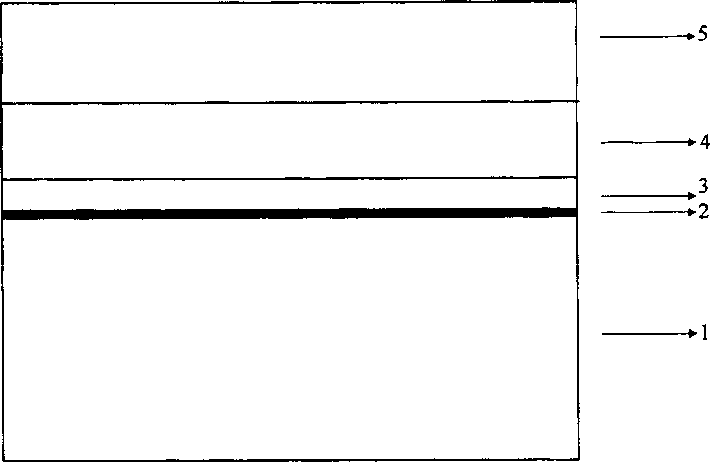
[0044] Take metal organic chemical vapor deposition (MOCVD) method as an example.

[0045] 1) Using the single crystal silicon (Si) (111) surface as the substrate;

[0046] 2) Raise the temperature to 1000~1100°C, pass through trimethylaluminum TMAl to form a thin aluminum (Al) layer on the silicon surface; then pass through ammonia to form an aluminum nitride (AlN) layer of about 30nm;

[0047] 3) The temperature is lowered to 800-1000° C., and an aluminum gallium nitride (AlGaN) stress compensation buffer layer is grown. Ammonia, trimethylgallium, and trimethylaluminum were used as raw material gases: the flow rate of ammonia was 4 L / min, the flow rate of trimethylgallium was 10 μmol / min, and the flow rate of trimethylaluminum was 10 μmol / min. At the same time, a small amount of indium (In) active agent is introduced. The thickness of this layer is 100nm;

[0048] 4) The temperature is raised to a high temperature of 1000~1100°C to grow a gallium nitride (GaN) epitaxial f...


PUM

PropertyMeasurementUnit
Thicknessaaaaaaaaaa

Abstract

The invention is a method for growing crackles family-III nitride on a silicon substrate, using stress compensating buffer layer to grow crackles a family-III nitride film on the silicon substrate, and comprising the steps of: 1) firstly depositing an about 20 nanometer thick aluminized high-temperature aluminum nitride buffer layer on a monocrystalline silicon substrate and then depositing a layer of hexagonal-phase matter (such as low-temperature aluminum nitride, gallium aluminum nitride or boron nitride) whose lattice constant is far less than that of the family-III nitride and thus forming a buffer layer with stress compensating function; and 2) adding in an activating agent to make a stress compensating layer easy to form at low temperature and simultaneously the surface smooth and the crystal quality high; 3) because the lattice constant of the predeposited hexagonal-phase matter is less than that of the family-III nitride, able to introduce pressure stress into the family-III nitride film grown on the predeposited hexagonal-phase matter so as to compensate drawing stress caused by mismatching with the silicon substrate.

Description

technical field [0001] The invention relates to the technical field of semiconductors, in particular to a method for preparing a crack-free silicon-based Group III nitride thin film for a stress compensation buffer layer. Background technique [0002] Group III nitride semiconductors represented by gallium nitride (GaN) have very broad applications because they can be used in blue LEDs and LDs, high-density optical storage, high-temperature, high-power and high-frequency electronic devices, and ultraviolet detectors. prospect. [0003] However, because there is no homogenous substrate, it is difficult to obtain high-quality gallium nitride (GaN) thin films. Most of the device-grade gallium nitride (GaN) films prepared so far are obtained on sapphire substrates. Because the sapphire substrate is hard, non-conductive, and expensive, it is difficult to produce in large quantities, forcing people to try to grow high-quality nitride on silicon substrates that are cheap, thermal...

Claims


Application Information

Patent Timeline
IPC IPC(8): H01L21/20
Inventor 吴洁君韩修训李杰民黎大兵陆沅王晓晖刘祥林王占国
Owner INST OF SEMICONDUCTORS - CHINESE ACAD OF SCI
Why Eureka
Try Eureka