Ferromagnetic/antiferromagnetic multilayer membrane material with pinning and its preparing method
An antiferromagnetic layer and antiferromagnetic technology, applied in spin-exchange coupled multilayer films, magnetic layers, substrate/intermediate layers, etc., can solve poor thermal stability, damage antiferromagnetic materials and even magnetic tunnel junction properties and other issues to achieve the effect of enhancing thermal stability
- Summary
- Abstract
- Description
- Claims
- Application Information
AI Technical Summary
Problems solved by technology
Method used
Image
Examples
Embodiment 1
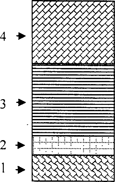
[0042] refer to Figure 2a Shown, the structure of the ferromagnetic / antiferromagnetic multilayer film that present embodiment makes is:
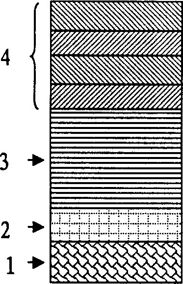
[0043] Glass is used as the substrate 1; a buffer layer 2 of Ta metal is set on the glass substrate 1, and the thickness of the buffer layer 2 is 4nm; a ferromagnetic layer Co is set on the buffer layer 2. 0.9 Fe 0.1 3. Its thickness is 12nm; an antiferromagnetic multilayer film [Pt / Cr 0.5 mn 0.5 ]4 set in the ferromagnetic layer Co 0.9 Fe 0.1 3, where Pt thickness is 1.26nm, Cr 0.5 mn 0.5 The thickness is 1nm, and the total thickness is about 27nm. At this time, Cr 0.5 mn 0.5 The atomic ratio to Pt is 1. The thickness or composition of each layer mentioned above is the value when the sample is vacuum-deposited.
Embodiment 2
[0045] Through the method of preparing ferromagnetic / antiferromagnetic multilayer film pinning system in this embodiment, it is beneficial to the preparation of Co-Fe ferromagnetic / Pt-Cr 0.5 mn 0.5 The structure of the antiferromagnetic multilayer pinning material is described in detail:
[0046] This embodiment prepares Co-Fe ferromagnetic / Pt-Cr 0.5 mn 0.5 The steps of antiferromagnetic multilayer film material are as follows:
[0047] 1). First use vacuum deposition coating method, such as magnetron sputtering method, the background vacuum degree is better than 10 -5 Pa, and the deposition working pressure under the inert atmosphere is 0.5Pa, on Si or glass substrate 1, coat Ta metal buffer layer 2 successively, the thickness of deposited Ta metal buffer layer 2 is 4nm, one Co 0.9 Fe 0.1 ferromagnetic layer 3, its Co 0.9 Fe 0.1 The thickness of the ferromagnetic layer 3 is 12nm, and a layer of multilayer film [Pt (thickness is 1.26nm) / Cr 0.5 mn 0.5 (thickness is 1nm...
Embodiment 3
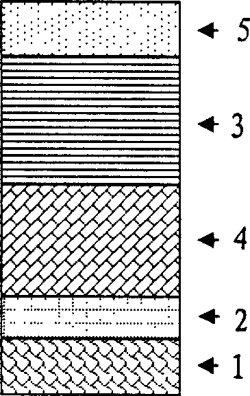
[0051] Such as Figure 2b As shown, the structure of preparing a ferromagnetic / antiferromagnetic multilayer film material with pinning is:
[0052] On the substrate 1 of glass, it is arranged in sequence; the buffer layer 2 of Ta metal has a thickness of 1nm; the antiferromagnetic layer multilayer film is [Pt / Cr 0.5 mn 0.5 ]4, where Pt thickness is 1.26nm, Cr 0.5 mn 0.5 The thickness is 1nm, and the total thickness is about 30nm. At this time, Cr 0.5 mn 0.5 The atomic ratio to Pt is 1; the ferromagnetic layer Co 0.9 Fe 0.1 3, its thickness is 12nm, and the protective layer 5 of Ta metal, its thickness is 3nm. The thickness or composition of each layer mentioned above is the value when the sample is vacuum-deposited. The magnetic properties of the sample in this embodiment are basically the same as those of the sample in Example 1.
[0053] The method of the ferromagnetic / antiferromagnetic multilayer film that present embodiment makes is as follows:
[0054] (1) Vacu...
PUM
| Property | Measurement | Unit |
|---|---|---|
| thickness | aaaaa | aaaaa |
| thickness | aaaaa | aaaaa |
| thickness | aaaaa | aaaaa |
Abstract
Description
Claims
Application Information


